ZHCSLO7B December 2020 – January 2023 LM25149-Q1
PRODUCTION DATA
- 1 特性
- 2 应用
- 3 说明
- 4 Revision History
- 5 说明(续)
- 6 Pin Configuration and Functions
- 7 Specifications
-
8 Detailed Description
- 8.1 Overview
- 8.2 Functional Block Diagram
- 8.3
Feature Description
- 8.3.1 Input Voltage Range (VIN)
- 8.3.2 High-Voltage Bias Supply Regulator (VCC, VCCX, VDDA)
- 8.3.3 Precision Enable (EN)
- 8.3.4 Power-Good Monitor (PG)
- 8.3.5 Switching Frequency (RT)
- 8.3.6 Active EMI Filter
- 8.3.7 Dual Random Spread Spectrum (DRSS)
- 8.3.8 Soft Start
- 8.3.9 Output Voltage Setpoint (FB)
- 8.3.10 Minimum Controllable On Time
- 8.3.11 Error Amplifier and PWM Comparator (FB, EXTCOMP)
- 8.3.12 Slope Compensation
- 8.3.13 Inductor Current Sense (ISNS+, VOUT)
- 8.3.14 Hiccup Mode Current Limiting
- 8.3.15 High-Side and Low-Side Gate Drivers (HO, LO)
- 8.3.16 Output Configurations (CNFG)
- 8.3.17 Single-Output Dual-Phase Operation
- 8.4 Device Functional Modes
-
9 Application and Implementation
- 9.1 Application Information
- 9.2
Typical Applications
- 9.2.1
Design 1 – High-Efficiency 2.1-MHz Synchronous
Buck Regulator
- 9.2.1.1 Design Requirements
- 9.2.1.2
Detailed Design Procedure
- 9.2.1.2.1 Custom Design With WEBENCH® Tools
- 9.2.1.2.2 Custom Design With Excel Quickstart Tool
- 9.2.1.2.3 Buck Inductor
- 9.2.1.2.4 Current-Sense Resistance
- 9.2.1.2.5 Output Capacitors
- 9.2.1.2.6 Input Capacitors
- 9.2.1.2.7 Frequency Set Resistor
- 9.2.1.2.8 Feedback Resistors
- 9.2.1.2.9 Compensation Components
- 9.2.1.2.10 Active EMI Components
- 9.2.1.3 Application Curves
- 9.2.2 Design 2 – High Efficiency 440-kHz Synchronous Buck Regulator
- 9.2.3 Design 3 – Dual-Phase 400-kHz 20-A Synchronous Buck Regulator
- 9.2.1
Design 1 – High-Efficiency 2.1-MHz Synchronous
Buck Regulator
- 9.3 Power Supply Recommendations
- 9.4 Layout
- 10Device and Documentation Support
- 11Mechanical, Packaging, and Orderable Information
8.3.3 Precision Enable (EN)
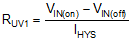
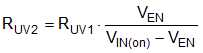
The EN pin can be connected to a voltage as high as 42 V. The LM25149-Q1 has a precision enable function. When the EN voltage is greater than 1 V, switching is enabled. If the EN pin is pulled below 0.5 V, the LM25149-Q1 is in shutdown with an IQ of 2.3 μA (typical) current drawn from VIN. When the EN voltage is between 0.5 V and 1 V, the LM25149-Q1 is in standby mode, the VCC regulator is active, and the controller is not switching. When the controller is in standby mode, the non-switching input quiescent current is 124 μA (typical). The LM25149-Q1 is enabled with a voltage greater than 1.0 V on the EN pin. However, many applications benefit from using a resistor divider RUV1 and RUV2, as shown in #GUID-BA6E3F7A-71C9-4DEE-8B91-204E6E989A6E, to establish a precision UVLO level. TI does not recommend leaving the EN pin floating.
Use #GUID-8B04AD33-A682-4F69-8263-607360A2A0CA and #GUID-7ED85693-5ACD-4E94-BD4A-DA81067FF7DB to calculate the UVLO resistors given the required input turn-on and turn-off voltages.