ZHCSLO7B December 2020 – January 2023 LM25149-Q1
PRODUCTION DATA
- 1 特性
- 2 应用
- 3 说明
- 4 Revision History
- 5 说明(续)
- 6 Pin Configuration and Functions
- 7 Specifications
-
8 Detailed Description
- 8.1 Overview
- 8.2 Functional Block Diagram
- 8.3
Feature Description
- 8.3.1 Input Voltage Range (VIN)
- 8.3.2 High-Voltage Bias Supply Regulator (VCC, VCCX, VDDA)
- 8.3.3 Precision Enable (EN)
- 8.3.4 Power-Good Monitor (PG)
- 8.3.5 Switching Frequency (RT)
- 8.3.6 Active EMI Filter
- 8.3.7 Dual Random Spread Spectrum (DRSS)
- 8.3.8 Soft Start
- 8.3.9 Output Voltage Setpoint (FB)
- 8.3.10 Minimum Controllable On Time
- 8.3.11 Error Amplifier and PWM Comparator (FB, EXTCOMP)
- 8.3.12 Slope Compensation
- 8.3.13 Inductor Current Sense (ISNS+, VOUT)
- 8.3.14 Hiccup Mode Current Limiting
- 8.3.15 High-Side and Low-Side Gate Drivers (HO, LO)
- 8.3.16 Output Configurations (CNFG)
- 8.3.17 Single-Output Dual-Phase Operation
- 8.4 Device Functional Modes
-
9 Application and Implementation
- 9.1 Application Information
- 9.2
Typical Applications
- 9.2.1
Design 1 – High-Efficiency 2.1-MHz Synchronous
Buck Regulator
- 9.2.1.1 Design Requirements
- 9.2.1.2
Detailed Design Procedure
- 9.2.1.2.1 Custom Design With WEBENCH® Tools
- 9.2.1.2.2 Custom Design With Excel Quickstart Tool
- 9.2.1.2.3 Buck Inductor
- 9.2.1.2.4 Current-Sense Resistance
- 9.2.1.2.5 Output Capacitors
- 9.2.1.2.6 Input Capacitors
- 9.2.1.2.7 Frequency Set Resistor
- 9.2.1.2.8 Feedback Resistors
- 9.2.1.2.9 Compensation Components
- 9.2.1.2.10 Active EMI Components
- 9.2.1.3 Application Curves
- 9.2.2 Design 2 – High Efficiency 440-kHz Synchronous Buck Regulator
- 9.2.3 Design 3 – Dual-Phase 400-kHz 20-A Synchronous Buck Regulator
- 9.2.1
Design 1 – High-Efficiency 2.1-MHz Synchronous
Buck Regulator
- 9.3 Power Supply Recommendations
- 9.4 Layout
- 10Device and Documentation Support
- 11Mechanical, Packaging, and Orderable Information
8.3.13.1 Shunt Current Sensing
#GUID-D3F5BF37-539D-4B9F-9FE7-343DE0BC522E illustrates inductor current sensing using a shunt resistor. This configuration
continuously monitors the inductor current to provide accurate overcurrent protection across
the operating temperature range. For optimal current sense accuracy and overcurrent
protection, use a low inductance ±1% tolerance shunt resistor between the inductor and
the output, with a Kelvin connection to the LM25149-Q1
current sense amplifier.
 Figure 8-5 Shunt Current Sensing
Implementation
Figure 8-5 Shunt Current Sensing
Implementation
If the peak voltage signal sensed from ISNS+ to VOUT exceeds the current limit threshold of 60 mV, the current limit comparator immediately terminates the HO output for cycle-by-cycle current limiting. Calculate the shunt resistance using #SNVSB297520.
Equation 10. 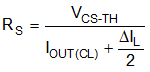
where
- VCS-TH is current sense threshold of 60 mV.
- IOUT(CL) is the overcurrent setpoint that is set higher than the maximum load current to avoid tripping the overcurrent comparator during load transients.
- ΔIL is the peak-to-peak inductor ripple current.
Figure 8-5 Shunt Current Sensing
ImplementationThe soft-start voltage is clamped 150 mV above FB during an overcurrent condition. Sixteen overcurrent events must occur before the SS clamp is enabled. This action makes sure that SS can be pulled low during brief overcurrent events, preventing output voltage overshoot during recovery.