ZHCSLO7B December 2020 – January 2023 LM25149-Q1
PRODUCTION DATA
- 1 特性
- 2 应用
- 3 说明
- 4 Revision History
- 5 说明(续)
- 6 Pin Configuration and Functions
- 7 Specifications
-
8 Detailed Description
- 8.1 Overview
- 8.2 Functional Block Diagram
- 8.3
Feature Description
- 8.3.1 Input Voltage Range (VIN)
- 8.3.2 High-Voltage Bias Supply Regulator (VCC, VCCX, VDDA)
- 8.3.3 Precision Enable (EN)
- 8.3.4 Power-Good Monitor (PG)
- 8.3.5 Switching Frequency (RT)
- 8.3.6 Active EMI Filter
- 8.3.7 Dual Random Spread Spectrum (DRSS)
- 8.3.8 Soft Start
- 8.3.9 Output Voltage Setpoint (FB)
- 8.3.10 Minimum Controllable On Time
- 8.3.11 Error Amplifier and PWM Comparator (FB, EXTCOMP)
- 8.3.12 Slope Compensation
- 8.3.13 Inductor Current Sense (ISNS+, VOUT)
- 8.3.14 Hiccup Mode Current Limiting
- 8.3.15 High-Side and Low-Side Gate Drivers (HO, LO)
- 8.3.16 Output Configurations (CNFG)
- 8.3.17 Single-Output Dual-Phase Operation
- 8.4 Device Functional Modes
-
9 Application and Implementation
- 9.1 Application Information
- 9.2
Typical Applications
- 9.2.1
Design 1 – High-Efficiency 2.1-MHz Synchronous
Buck Regulator
- 9.2.1.1 Design Requirements
- 9.2.1.2
Detailed Design Procedure
- 9.2.1.2.1 Custom Design With WEBENCH® Tools
- 9.2.1.2.2 Custom Design With Excel Quickstart Tool
- 9.2.1.2.3 Buck Inductor
- 9.2.1.2.4 Current-Sense Resistance
- 9.2.1.2.5 Output Capacitors
- 9.2.1.2.6 Input Capacitors
- 9.2.1.2.7 Frequency Set Resistor
- 9.2.1.2.8 Feedback Resistors
- 9.2.1.2.9 Compensation Components
- 9.2.1.2.10 Active EMI Components
- 9.2.1.3 Application Curves
- 9.2.2 Design 2 – High Efficiency 440-kHz Synchronous Buck Regulator
- 9.2.3 Design 3 – Dual-Phase 400-kHz 20-A Synchronous Buck Regulator
- 9.2.1
Design 1 – High-Efficiency 2.1-MHz Synchronous
Buck Regulator
- 9.3 Power Supply Recommendations
- 9.4 Layout
- 10Device and Documentation Support
- 11Mechanical, Packaging, and Orderable Information
9.2.1.2.5 Output Capacitors
- Use Equation 39 to estimate the output capacitance required to manage the output voltage overshoot
during a load-off transient (from full load to no load) assuming a load transient
deviation specification of 1.5% (75 mV for a 5-V output). Equation 39.
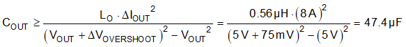
- Noting the voltage coefficient of ceramic capacitors where the effective capacitance decreases significantly with applied voltage, select four 47-µF, 10-V, X7R, 1210 ceramic output capacitors. Generally, when sufficient capacitance is used to satisfy the load-off transient response requirement, the voltage undershoot during a no-load to full-load transient is also satisfactory.
- Use Equation 40 to estimate the peak-peak output voltage ripple at nominal input voltage.
Equation 40.

where
- RESR is the effective equivalent series resistance (ESR) of the output capacitors.
- 44 µF is the total effective (derated) ceramic output capacitance at 5 V.
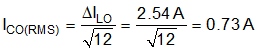
- Use Equation 41 to calculate the output capacitor RMS ripple current using and verify that the ripple current is within the capacitor ripple current rating.
Equation 41.