ZHCSLO7B December 2020 – January 2023 LM25149-Q1
PRODUCTION DATA
- 1 特性
- 2 应用
- 3 说明
- 4 Revision History
- 5 说明(续)
- 6 Pin Configuration and Functions
- 7 Specifications
-
8 Detailed Description
- 8.1 Overview
- 8.2 Functional Block Diagram
- 8.3
Feature Description
- 8.3.1 Input Voltage Range (VIN)
- 8.3.2 High-Voltage Bias Supply Regulator (VCC, VCCX, VDDA)
- 8.3.3 Precision Enable (EN)
- 8.3.4 Power-Good Monitor (PG)
- 8.3.5 Switching Frequency (RT)
- 8.3.6 Active EMI Filter
- 8.3.7 Dual Random Spread Spectrum (DRSS)
- 8.3.8 Soft Start
- 8.3.9 Output Voltage Setpoint (FB)
- 8.3.10 Minimum Controllable On Time
- 8.3.11 Error Amplifier and PWM Comparator (FB, EXTCOMP)
- 8.3.12 Slope Compensation
- 8.3.13 Inductor Current Sense (ISNS+, VOUT)
- 8.3.14 Hiccup Mode Current Limiting
- 8.3.15 High-Side and Low-Side Gate Drivers (HO, LO)
- 8.3.16 Output Configurations (CNFG)
- 8.3.17 Single-Output Dual-Phase Operation
- 8.4 Device Functional Modes
-
9 Application and Implementation
- 9.1 Application Information
- 9.2
Typical Applications
- 9.2.1
Design 1 – High-Efficiency 2.1-MHz Synchronous
Buck Regulator
- 9.2.1.1 Design Requirements
- 9.2.1.2
Detailed Design Procedure
- 9.2.1.2.1 Custom Design With WEBENCH® Tools
- 9.2.1.2.2 Custom Design With Excel Quickstart Tool
- 9.2.1.2.3 Buck Inductor
- 9.2.1.2.4 Current-Sense Resistance
- 9.2.1.2.5 Output Capacitors
- 9.2.1.2.6 Input Capacitors
- 9.2.1.2.7 Frequency Set Resistor
- 9.2.1.2.8 Feedback Resistors
- 9.2.1.2.9 Compensation Components
- 9.2.1.2.10 Active EMI Components
- 9.2.1.3 Application Curves
- 9.2.2 Design 2 – High Efficiency 440-kHz Synchronous Buck Regulator
- 9.2.3 Design 3 – Dual-Phase 400-kHz 20-A Synchronous Buck Regulator
- 9.2.1
Design 1 – High-Efficiency 2.1-MHz Synchronous
Buck Regulator
- 9.3 Power Supply Recommendations
- 9.4 Layout
- 10Device and Documentation Support
- 11Mechanical, Packaging, and Orderable Information
9.2.1.2.4 Current-Sense Resistance
- Calculate the current-sense resistance based on a
maximum peak current capability of at least 25% higher than the peak inductor
current at full load to provide sufficient margin during start-up and load-on
transients. Calculate the current sense resistances using Equation 37. Equation 37.
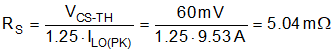
where
- VCS-TH is the 60-mV current limit threshold.
- Select a standard resistance value of 5 mΩ for the shunt. An 0508 footprint component with wide aspect ratio termination design provides 1-W power rating, low parasitic series inductance, and compact PCB layout. Carefully adhere to the layout guidelines in GUID-BFD90C37-2547-45D4-942D-126A85B9F387.html#GUID-BFD90C37-2547-45D4-942D-126A85B9F387 to make sure that noise and DC errors do not corrupt the differential current-sense voltages measured at the ISNS+ and VOUT pins.
- Place the shunt resistor close to the inductor.
- Use Kelvin-sense connections, and route the sense lines differentially from the shunt to the LM25149-Q1.
- The CS-to-output propagation delay (related to
the current limit comparator, internal logic, and power MOSFET gate drivers)
causes the peak current to increase above the calculated current limit
threshold. For a total propagation delay tDELAY-ISNS+ of 40 ns, use
Equation 38 to calculate the worst-case peak inductor current with the output shorted.
Equation 38.

- Based on this result, select an inductor with saturation current greater than 16 A across the full operating temperature range.