ZHCSTL8F April 2007 – November 2023 LM25116
PRODUCTION DATA
- 1
- 1 特性
- 2 应用
- 3 说明
- 4 Pin Configuration and Functions
- 5 Specifications
- 6 Detailed Description
-
7 Application and Implementation
- 7.1 Application Information
- 7.2
Typical Application
- 7.2.1 Design Requirements
- 7.2.2
Detailed Design Procedure
- 7.2.2.1 Timing Resistor
- 7.2.2.2 Output Inductor
- 7.2.2.3 Current Sense Resistor
- 7.2.2.4 Ramp Capacitor
- 7.2.2.5 Output Capacitors
- 7.2.2.6 Input Capacitors
- 7.2.2.7 VCC Capacitor
- 7.2.2.8 Bootstrap Capacitor
- 7.2.2.9 Soft Start Capacitor
- 7.2.2.10 Output Voltage Divider
- 7.2.2.11 UVLO Divider
- 7.2.2.12 MOSFETs
- 7.2.2.13 MOSFET Snubber
- 7.2.2.14 Error Amplifier Compensation
- 7.2.2.15 Comprehensive Equations
- 7.2.3 Application Curves
- 7.3 Power Supply Recommendations
- 7.4 Layout
- 8 Device and Documentation Support
- 9 Revision History
- 10Mechanical, Packaging, and Orderable Information
7.2.2.2 Output Inductor
The inductor value is determined based on the operating frequency, load current, ripple current and the input and output voltages.
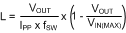
 Figure 7-2 Inductor Current
Knowing the switching frequency (fSW), maximum ripple current (IPP), maximum input voltage (VIN(MAX)) and the nominal output voltage (VOUT), the inductor value is calculated with Equation 8.
The maximum ripple current occurs at the maximum input voltage. Typically, IPP is 20% to 40% of the full load current. When running diode emulation mode, the maximum ripple current must be less than twice the minimum load current. For full synchronous operation, higher ripple current is acceptable. Higher ripple current allows for a smaller inductor size, but places more of a burden on the output capacitor to smooth the ripple current for low output ripple voltage. For this example, 40% ripple current is chosen for a smaller sized inductor in Equation 9.
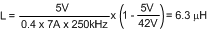
The nearest standard value of 6 µH is used. The inductor must be rated for the peak current to prevent saturation. During normal operation, the peak current occurs at maximum load current plus maximum ripple. During overload conditions with properly scaled component values, the peak current is limited to VCS(TH) / RS (See Section 7.2.2.3). At the maximum input voltage with a shorted output, the valley current must fall below VCS(TH) / RS before the high-side MOSFET is allowed to turn on. The peak current in steady state increases to VIN(MAX) x tON(min) / L above this level. The chosen inductor must be evaluated for this condition, especially at elevated temperature where the saturation current rating may drop significantly.