ZHCSTL8F April 2007 – November 2023 LM25116
PRODUCTION DATA
- 1
- 1 特性
- 2 应用
- 3 说明
- 4 Pin Configuration and Functions
- 5 Specifications
- 6 Detailed Description
-
7 Application and Implementation
- 7.1 Application Information
- 7.2
Typical Application
- 7.2.1 Design Requirements
- 7.2.2
Detailed Design Procedure
- 7.2.2.1 Timing Resistor
- 7.2.2.2 Output Inductor
- 7.2.2.3 Current Sense Resistor
- 7.2.2.4 Ramp Capacitor
- 7.2.2.5 Output Capacitors
- 7.2.2.6 Input Capacitors
- 7.2.2.7 VCC Capacitor
- 7.2.2.8 Bootstrap Capacitor
- 7.2.2.9 Soft Start Capacitor
- 7.2.2.10 Output Voltage Divider
- 7.2.2.11 UVLO Divider
- 7.2.2.12 MOSFETs
- 7.2.2.13 MOSFET Snubber
- 7.2.2.14 Error Amplifier Compensation
- 7.2.2.15 Comprehensive Equations
- 7.2.3 Application Curves
- 7.3 Power Supply Recommendations
- 7.4 Layout
- 8 Device and Documentation Support
- 9 Revision History
- 10Mechanical, Packaging, and Orderable Information
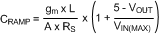
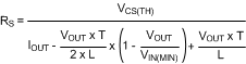
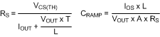
7.2.2.15.1 Current Sense Resistor and Ramp Capacitor
T = 1 / fSW, gm = 5 µA/V, A = 10 V/V. IOUT is the maximum output current at current limit.
General method for VOUT < 5 V is Equation 35 and Equation 36.
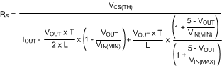
General method for 5 V < VOUT < 7.5 V is Equation 37 and Equation 38.
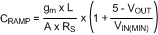
Best performance method minimizes the current limit deviation due to changes in line voltage, while maintaining near optimal slope compensation.
Calculate optimal slope current with Equation 39, IOS = (VOUT / 3) × 10 µA/V. For example, at VOUT = 7.5 V,
IOS = 25 µA.
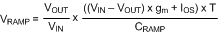
Calculate VRAMP at the nominal input voltage with Equation 40.
For VOUT > 7.5 V, install a resistor from the RAMP pin to VCC and calculate with Equation 41.
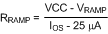
 Figure 7-6 RRAMP to VCC for VOUT > 7.5 V
For VOUT < 7.5 V, a negative VCC is required. This can be made with a simple charge pump from the LO gate output. Install a resistor from the RAMP pin to the negative VCC and calculate with Equation 42.
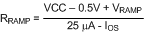
 Figure 7-7 RRAMP to –VCC for VOUT < 7.5 V
If a large variation is expected in VCC, say for VIN < 11 V, a Zener regulator may be added to supply a constant voltage for RRAMP.