ZHCSTL8F April 2007 – November 2023 LM25116
PRODUCTION DATA
- 1
- 1 特性
- 2 应用
- 3 说明
- 4 Pin Configuration and Functions
- 5 Specifications
- 6 Detailed Description
-
7 Application and Implementation
- 7.1 Application Information
- 7.2
Typical Application
- 7.2.1 Design Requirements
- 7.2.2
Detailed Design Procedure
- 7.2.2.1 Timing Resistor
- 7.2.2.2 Output Inductor
- 7.2.2.3 Current Sense Resistor
- 7.2.2.4 Ramp Capacitor
- 7.2.2.5 Output Capacitors
- 7.2.2.6 Input Capacitors
- 7.2.2.7 VCC Capacitor
- 7.2.2.8 Bootstrap Capacitor
- 7.2.2.9 Soft Start Capacitor
- 7.2.2.10 Output Voltage Divider
- 7.2.2.11 UVLO Divider
- 7.2.2.12 MOSFETs
- 7.2.2.13 MOSFET Snubber
- 7.2.2.14 Error Amplifier Compensation
- 7.2.2.15 Comprehensive Equations
- 7.2.3 Application Curves
- 7.3 Power Supply Recommendations
- 7.4 Layout
- 8 Device and Documentation Support
- 9 Revision History
- 10Mechanical, Packaging, and Orderable Information
6.3.1 High-Voltage Start-Up Regulator
The LM25116 contains a dual mode internal high-voltage start-up regulator that provides the VCC bias supply for the PWM controller and a bootstrap gate drive for the high-side buck MOSFET. The input pin (VIN) can be connected directly to an input voltage source as high as 42 V. For input voltages below 10.6 V, a low dropout switch connects VCC directly to VIN. In this supply range, VCC is approximately equal to VIN. For VIN voltages greater than 10.6 V, the low dropout switch is disabled and the VCC regulator is enabled to maintain VCC at approximately 7.4 V. The wide operating range of 6 V to 42 V is achieved through the use of this dual mode regulator.
Upon power up, the regulator sources current into the capacitor connected to the VCC pin. When the voltage at the VCC pin exceeds 4.5 V and the UVLO pin is greater than 1.215 V, the output switch is enabled and a soft-start sequence begins. The output switch remains enabled until VCC falls below 4.5 V, EN is pulled low, the UVLO pin falls below 1.215 V, or the die temperature exceeds the thermal limit threshold.
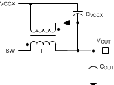
 Figure 6-1 VCCX Bias Supply with Additional Inductor Winding
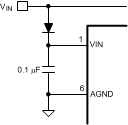
An output voltage derived bias supply can be applied to the VCCX pin to reduce the IC power dissipation. If the bias supply voltage is greater than 4.5 V, the internal regulator essentially shuts off, reducing the IC power dissipation. The VCC regulator series pass transistor includes a diode between VCC and VIN that must not be forward biased in normal operation. For an output voltage between 5 V and 15 V, VOUT can be connected directly to VCCX. For VOUT < 5 V, a bias winding on the output inductor can be added to VOUT. If the bias winding can supply VCCX greater than VIN, an external blocking diode is required from the input power supply to the VIN pin to prevent VCC from discharging into the input supply.
The output of the VCC regulator is current limited to 15 mA minimum. The VCC current is determined by the MOSFET gate charge, switching frequency and quiescent current (see Section 7.2.2.12 in the Section 7.2). If VCCX is powered by the output voltage or an inductor winding, the VCC current must be evaluated during start-up to ensure that it is less than the 15 mA minimum current limit specification. If VCCX is powered by an external regulator derived from VIN, there is no restriction on the VCC current.
 Figure 6-2 Input Blocking Diode for VCCX > VIN
In high-voltage applications, take extra care to ensure the VIN pin does not exceed the absolute maximum voltage rating of 45 V. During line or load transients, voltage ringing on the VIN line that exceeds values listed in Section 5.1 can damage the IC. Both careful PCB layout and the use of quality bypass capacitors placed close to the VIN and GND pins are essential.