ZHCSJS5D March 2011 – May 2019 LM21215A
PRODUCTION DATA.
- 1 特性
- 2 应用
- 3 说明
- 4 修订历史记录
- 5 Pin Configuration and Functions
- 6 Specifications
- 7 Detailed Description
- 8 Application and Implementation
- 9 Power Supply Recommendations
- 10Layout
- 11器件和文档支持
- 12机械、封装和可订购信息
10.1.1 Compact PCB Layout for EMI Reduction
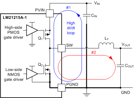
Radiated EMI generated by high di/dt components relates to pulsing currents in switching converters. The larger area covered by the path of a pulsing current, the more electromagnetic emission is generated. The key to reducing radiated EMI is to identify the pulsing current path and minimize the area of that path. The main switching loop of the LM21215A power stage is denoted by #1 in Figure 41. The topological architecture of a buck converter means that particularly high di/dt current flows in loop #1, and it becomes mandatory to reduce the parasitic inductance of this loop by minimizing its effective loop area. For loop #2 however, the di/dt through inductor LF and capacitor COUT is naturally limited by the inductor. Keeping the area of loop #2 small is not nearly as important as that of loop #1. Also important are the gate drive loops of the low-side and high-side MOSFETs, which are inherently tight by virtue of the integrated power MOSFETs and gate drivers of the LM21215A
 Figure 41. LM21215A Power Stage Circuit Switching Loops
 High-frequency ceramic bypass capacitors at the input side provide the primary path for the high di/dt components of the pulsing current. Placing ceramic bypass capacitors as close as possible to the PVIN and PGND pins is the key to EMI reduction. Keep the SW trace connecting to the inductor as short as possible, and just wide enough to carry the load current without excessive heating. Use short, thick traces or copper pours (shapes) for current conduction path to minimize parasitic resistance. Place the output capacitors close to the VOUT side of the inductor and route the return using GND plane copper back to the PGND pins and the exposed pad of the LM21215A.