ZHCSJS5D March   2011  – May 2019 LM21215A

PRODUCTION DATA.  

  1. 特性
  2. 应用
    1.     2.5V、500kHz 时的效率
  3. 说明
    1.     典型应用电路
      1.      Device Images
  4. 修订历史记录
  5. Pin Configuration and Functions
    1.     Pin Functions
  6. Specifications
    1. 6.1 Absolute Maximum Ratings
    2. 6.2 ESD Ratings
    3. 6.3 Recommended Operating Conditions
    4. 6.4 Thermal Information
    5. 6.5 Electrical Characteristics
    6. 6.6 Typical Characteristics
  7. Detailed Description
    1. 7.1 Overview
    2. 7.2 Functional Block Diagram
    3. 7.3 Feature Description
      1. 7.3.1 Precision Enable
      2. 7.3.2 Input Voltage UVLO
      3. 7.3.3 Soft-Start Capability
      4. 7.3.4 PGOOD Indicator
      5. 7.3.5 Frequency Synchronization
      6. 7.3.6 Current Limit
      7. 7.3.7 Short Circuit Protection
    4. 7.4 Device Functional Modes
      1. 7.4.1 Light-Load Operation
      2. 7.4.2 Overvoltage and Undervoltage Handling
      3. 7.4.3 Thermal Shutdown
  8. Application and Implementation
    1. 8.1 Application Information
    2. 8.2 Typical Applications
      1. 8.2.1 Typical Application 1
        1. 8.2.1.1 Design Requirements
        2. 8.2.1.2 Detailed Design Procedure
          1. 8.2.1.2.1 Custom Design With WEBENCH® Tools
          2. 8.2.1.2.2 Output Voltage Setpoint
          3. 8.2.1.2.3 Precision Enable
          4. 8.2.1.2.4 Filter Inductor Selection
          5. 8.2.1.2.5 Output Capacitor Selection
          6. 8.2.1.2.6 Input Capacitor Selection
          7. 8.2.1.2.7 Control Loop Compensation
        3. 8.2.1.3 Application Curves
      2. 8.2.2 Typical Application 2
        1. 8.2.2.1 Design Requirements
        2. 8.2.2.2 Detailed Design Procedure
  9. Power Supply Recommendations
  10. 10Layout
    1. 10.1 Layout Guidelines
      1. 10.1.1 Compact PCB Layout for EMI Reduction
      2. 10.1.2 Thermal Design
      3. 10.1.3 Ground Plane Design
    2. 10.2 Layout Example
  11. 11器件和文档支持
    1. 11.1 器件支持
      1. 11.1.1 第三方产品免责声明
      2. 11.1.2 开发支持
        1. 11.1.2.1 使用 WEBENCH® 工具创建定制设计方案
    2. 11.2 文档支持
      1. 11.2.1 相关文档
    3. 11.3 社区资源
    4. 11.4 商标
    5. 11.5 静电放电警告
    6. 11.6 Glossary
  12. 12机械、封装和可订购信息

封装选项

机械数据 (封装 | 引脚)
散热焊盘机械数据 (封装 | 引脚)
订购信息

Precision Enable

The Enable (EN) pin of the LM21215A allows the output to be toggled on and off. This pin is a precision analog input. When the voltage exceeds 1.35 V, the converter begins to regulate the output voltage as long as AVIN has exceeded the UVLO threshold voltage of 2.7 V. There is an internal pullup current source of 2 µA connected to EN. If enable is not used, the device turns on automatically. Also, if EN is not toggled directly, the device can be set to turn on at a certain input voltage higher than the internal UVLO rising threshold. This is achieved with an external resistor divider from AVIN to EN and EN to AGND as shown in Figure 30.
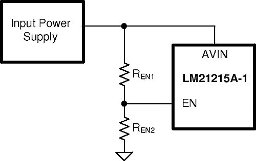
LM21215A enable_nosb87.gifFigure 30. Input Voltage Turn-on Setpoint Configured by Enable Resistor Divider

The resistances of REN1 and REN2 are chosen to allow EN to reach its rising threshold voltage at the desired the input supply voltage. With the enable current source included, use Equation 4 to solve for REN1.

Equation 4. LM21215A q_Ren1_nosb87.gif

where

  • REN1 is the resistor from VIN to EN
  • REN2 is the resistor from EN to AGND
  • IEN is the internal enable pullup current (2 µA)
  • 1.35 V is the precision enable rising threshold voltage

Typical values for REN2 range from 10 kΩ to 100 kΩ.