ZHCSND8 april 2021 LM117QML-SP
PRODUCTION DATA
- 1 特性
- 2 应用
- 3 说明
- 4 Revision History
- 5 Device Comparison Table
- 6 Pin Configurations and Functions
-
7 Specifications
- 7.1 Absolute Maximum Ratings
- 7.2 ESD Ratings
- 7.3 Recommended Operating Conditions
- 7.4 Thermal Information
- 7.5 Electrical Characteristics: 0.5–A IOUT Devices (LM117H, LM117GW)
- 7.6 Parameter Drift: 0.5–A IOUT Devices (LM117H, LM117GW)
- 7.7 Electrical Characteristics: 1.5–A IOUT Devices (LM117K)
- 7.8 Parameter Drift: 1.5–A IOUT Devices (LM117K)
- 7.9 Quality Conformance Inspection
- 7.10 Typical Characteristics
- 8 Detailed Description
- 9 Application and Implementation
- 10Power Supply Recommendations
- 11Layout
- 12Device and Documentation Support
封装选项
机械数据 (封装 | 引脚)
散热焊盘机械数据 (封装 | 引脚)
订购信息
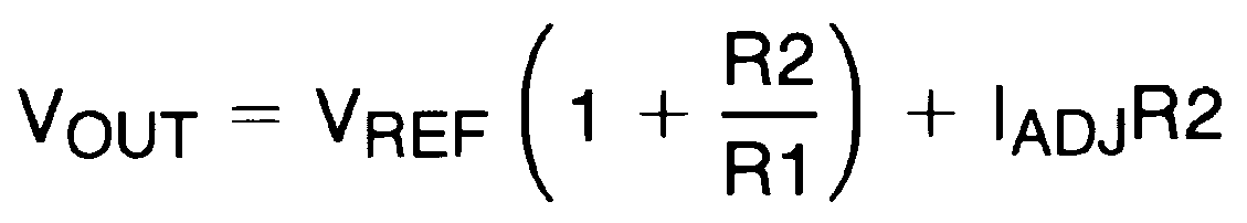
8.3 Setting Output Voltage
In operation, the LM117 develops a nominal 1.25-V reference voltage, VREF, between the output and adjustment terminal. The reference voltage is expressed across R1 and, since the voltage is constant, a constant current I1 then flows through R2, giving an output voltage found by using Equation 1.
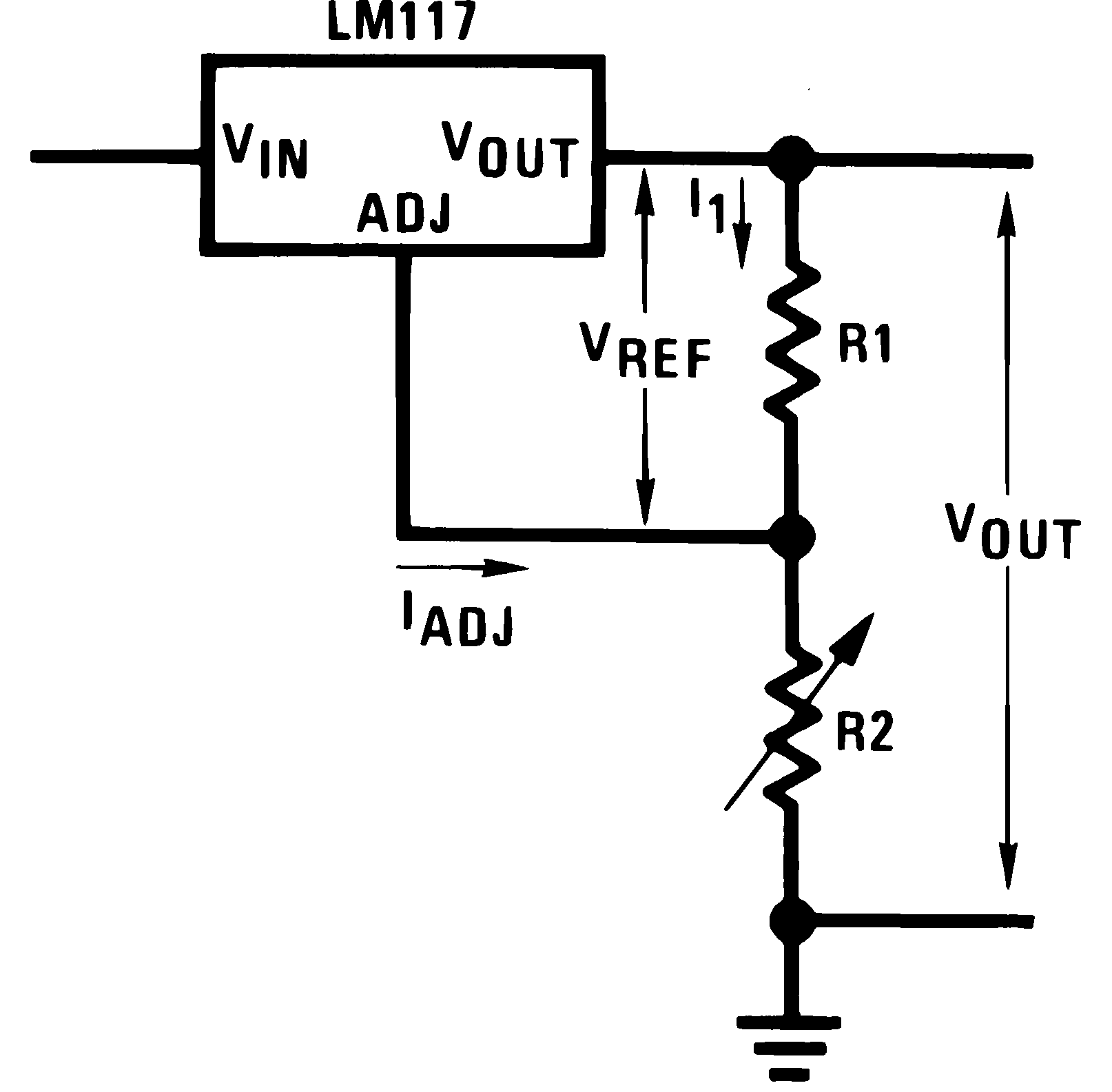
Since the 100-μA current from the adjustment terminal represents an error term, the LM117 was designed to minimize IADJ and make it relatively constant with line and load changes. To do this, all quiescent operating current is returned to the output establishing a minimum load current requirement. If there is insufficient load on the output, the output will rise.
To mitigate the requirement for an added load to sink the required output current, the resistor divider may be selected so that it alone can sink the largest specified output load current of 5 mA. This has the additional benefit of minimizing the IADJ error term (which varies over temperature).