ZHCSI90E December 2017 – October 2019 ISO1042
PRODUCTION DATA.
- 1 特性
- 2 应用
- 3 说明
- 4 修订历史记录
- 5 Pin Configuration and Functions
-
6 Specifications
- 6.1 Absolute Maximum Ratings
- 6.2 ESD Ratings
- 6.3 Transient Immunity
- 6.4 Recommended Operating Conditions
- 6.5 Thermal Information
- 6.6 Power Ratings
- 6.7 Insulation Specifications
- 6.8 Safety-Related Certifications
- 6.9 Safety Limiting Values
- 6.10 Electrical Characteristics - DC Specification
- 6.11 Switching Characteristics
- 6.12 Insulation Characteristics Curves
- 6.13 Typical Characteristics
- 7 Parameter Measurement Information
- 8 Detailed Description
- 9 Application and Implementation
- 10Power Supply Recommendations
- 11Layout
- 12器件和文档支持
- 13机械、封装和可订购信息
封装选项
请参考 PDF 数据表获取器件具体的封装图。
机械数据 (封装 | 引脚)
- DWV|8
- DW|16
散热焊盘机械数据 (封装 | 引脚)
- DW|16
订购信息
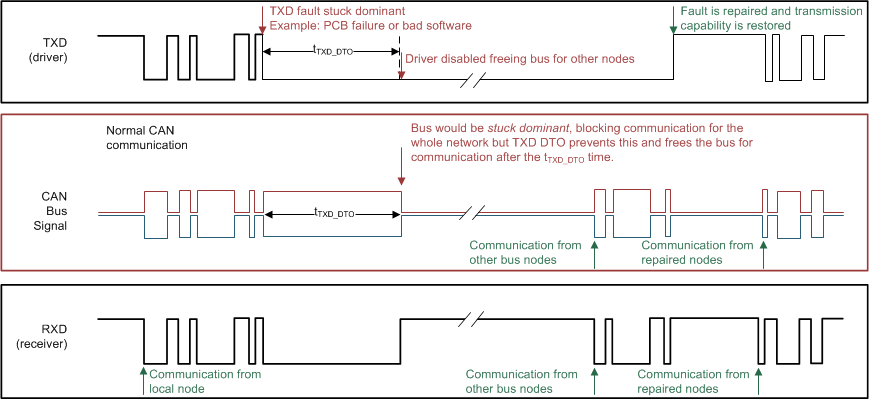
8.3.3.1 TXD Dominant Timeout (DTO)
The TXD DTO circuit prevents the transceiver from blocking network communication in the event of a hardware or software failure where the TXD pin is held dominant longer than the timeout period, tTXD_DTO. The DTO circuit timer starts on a falling edge on the TXD pin. The DTO circuit disables the CAN bus driver if no rising edge occurs before the timeout period expires, which frees the bus for communication between other nodes on the network. The CAN driver is activated again when a recessive signal occurs on the TXD pin, clearing the TXD DTO condition. The receiver and RXD pin still reflect activity on the CAN bus, and the bus terminals are biased to the recessive level during a TXD dominant timeout.
 Figure 27. Example Timing Diagram for TXD DTO
 NOTE
The minimum dominant TXD time (tTXD_DTO) allowed by the TXD DTO circuit limits the minimum possible transmitted data rate of the device. The CAN protocol allows a maximum of eleven successive dominant bits (on TXD) for the worst case, where five successive dominant bits are followed immediately by an error frame. This, along with the tTXD_DTO minimum, limits the minimum data rate. Calculate the minimum transmitted data rate with Equation 1.