ZHCS968B June 2012 – November 2017 INA827
PRODUCTION DATA.
- 1 特性
- 2 应用
- 3 说明
- 4 修订历史记录
- 5 Pin Configuration and Functions
- 6 Specifications
- 7 Typical Characteristics
- 8 Detailed Description
- 9 Application and Implementation
- 10Power Supply Recommendations
- 11Layout
- 12器件和文档支持
- 13机械、封装和可订购信息
8.3.7 Reference Pin
The INA827 output voltage is developed with respect to the voltage on the reference pin. Often, in dual-supply operation, the reference pin (pin 6) is connected to the low-impedance system ground. Offsetting the output signal to a precise mid-supply level (for example, 2.5 V in a 5-V supply environment) can be useful in single-supply operation. The signal can be shifted by applying a voltage to the device REF pin, which can be useful when driving a single-supply ADC.
For best performance, keep any source impedance to the REF pin below 5 Ω. Referring to Figure 61, the reference resistor is at one end of a 50-kΩ resistor. Additional impedance at the REF pin adds to this 50-kΩ resistor. The imbalance in resistor ratios results in degraded common-mode rejection ratio (CMRR).
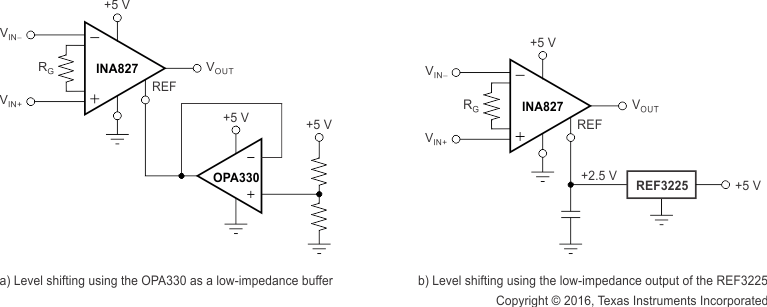
Figure 59 shows two different methods of driving the reference pin with low impedance. The OPA330 is a low-power, chopper-stabilized amplifier and therefore offers excellent stability over temperature. The OPA330 is available in the space-saving SC70 and even smaller chip-scale package. The REF3225 is a precision reference in a small SOT23-6 package.
 Figure 59. Options for Low-Impedance Level Shifting