ZHCSNH8B July 2021 – November 2021 INA823
PRODUCTION DATA
- 1 特性
- 2 应用
- 3 说明
- 4 Revision History
- 5 Device Comparison Table
- 6 Pin Configuration and Functions
- 7 Specifications
- 8 Detailed Description
- 9 Application and Implementation
- 10Power Supply Recommendations
- 11Layout
- 12Device and Documentation Support
- 13Mechanical, Packaging, and Orderable Information
9.2.1.2 Detailed Design Procedure
This section provides basic calculations to lay out the instrumentation amplifier with respect to the given design requirements.
One of the key considerations in resistive-bridge sensors is the common-mode voltage, VCM. If the bridge is balanced (no pressure, thus no voltage change), VCM(MAX) is half of the bridge excitation (VEXT). As the pressure increases to the maximum value, the common-mode voltage decreases to VCM(MIN).
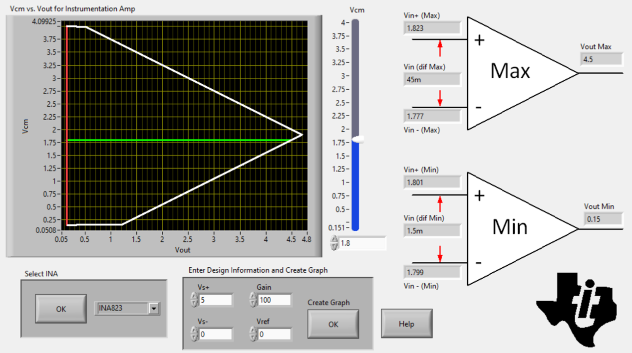
To achieve the output voltage of VOUT = 4.5 V with the INA823, the limitation for the common-mode voltage is at VCM(INA823max) = 1.8 V, as shown in Figure 7-56 and Figure 9-3 (where an initial gain value of 100 V/V is used as an approximation). An additional series resistor in the Wheatstone bridge string (R1) is required to shift the common-mode voltage to this value. However, be aware that shifting the common-mode voltage also changes the effective excitation voltage VEXT across the bridge.
 Figure 9-3 Screen Shot From Analog
Engineer's Calculator
Figure 9-3 Screen Shot From Analog
Engineer's CalculatorCalculate the new effective excitation voltage VEXT(NOM) associated with a desired VCM(MIN) value by solving the following:
VEXT(NOM) can in turn be used to calculate the desired value of R1:
Use a standard 0.1% resistor value of 4.12 kΩ.
Calculate the maximum value of VDIFF by solving the following equation for the maximum pressure of 10 psi:
Use the resulting value to verify that the minimum bridge common-mode voltage, VCM(MIN), is within the limits of the INA823 by solving the following:
Next, use Equation 7 to calculate the required gain for the given maximum sensor output voltage span, VDIFF, with respect to the required VOUT, which is the full-scale range of the ADC.
Equation 8 calculates the gain-setting resistor value using the INA823 gain equation shown in Equation 2:
Use a standard 0.1% resistor value of 768 Ω, so as not to exceed the full-scale range of the ADC.