ZHCSNH8B July 2021 – November 2021 INA823
PRODUCTION DATA
- 1 特性
- 2 应用
- 3 说明
- 4 Revision History
- 5 Device Comparison Table
- 6 Pin Configuration and Functions
- 7 Specifications
- 8 Detailed Description
- 9 Application and Implementation
- 10Power Supply Recommendations
- 11Layout
- 12Device and Documentation Support
- 13Mechanical, Packaging, and Orderable Information
9.1.1 Input Bias Current Return Path
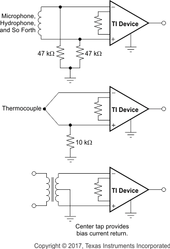
The input impedance of the INA823 is extremely high, but a path must be provided for the input bias current of both inputs. This input bias current is typically 1.2 nA. High input impedance means that this input bias current changes little with varying input voltage.
For proper operation, input circuitry must provide a path for this input bias current. Figure 9-1 shows various provisions for an input bias current path. Without a bias current path, the inputs float to a potential that exceeds the common-mode range of the INA823, and the input amplifiers saturate. If the differential source resistance is low, the bias current return path connects to one input (as shown in the thermocouple example in Figure 9-1). With a higher source impedance, use two equal resistors to provide a balanced input, with the possible advantages of a lower input offset voltage as a result of bias current, and better high-frequency common-mode rejection. Furthermore, matched input impedances generally minimize the impact to performance in cases where the input common-mode voltage is very low and input bias current can increase as the IB cancellation circuity runs out of headroom. The input offset current typically remains low; therefore, well-matched input impedances reduce the differential error voltage that would otherwise arise.
For more details about why a valid input bias current return path is necessary, see the Importance of Input Bias Current Return Paths in Instrumentation Amplifier Applications application note.
 Figure 9-1 Providing
an Input Common-Mode Current Path