ZHCSIM8C August 2018 – July 2019 INA821
PRODUCTION DATA.
- 1 特性
- 2 应用
- 3 说明
- 4 修订历史记录
- 5 Device Comparison Table
- 6 Pin Configuration and Functions
- 7 Specifications
- 8 Detailed Description
- 9 Application and Implementation
- 10Power Supply Recommendations
- 11Layout
- 12器件和文档支持
- 13机械、封装和可订购信息
封装选项
机械数据 (封装 | 引脚)
散热焊盘机械数据 (封装 | 引脚)
- DRG|8
订购信息
9.1.1 Reference Pin
The output voltage of the INA821 is developed with respect to the voltage on the reference pin (REF.) Often, in dual-supply operation, REF (pin 6) connects to the low-impedance system ground. In single-supply operation, offsetting the output signal to a precise midsupply level is useful (for example, 2.5 V in a 5-V supply environment). To accomplish this level shift, a voltage source must be connected to the REF pin to level-shift the output so that the INA821 drives a single-supply analog-to-digital converter (ADC).
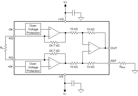
The voltage source applied to the reference pin must have a low output impedance. As shown in Figure 65, any resistance at the reference pin ( RREF in Figure 65) is in series with one of the internal 10-kΩ resistors.
 Figure 65. Parasitic Resistance Shown at the Reference Pin
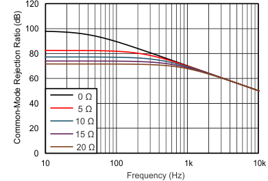
 The parasitic resistance at the reference pin (RREF) creates an imbalance in the four resistors of the internal difference amplifier that results in a degraded common-mode rejection ratio (CMRR). Figure 66 shows the degradation in CMRR of the INA821 as a result of the increased resistance at the reference pin. For the best performance, keep the source impedance to the REF pin (RREF) less than 5 Ω.
 Figure 66. The Effect of Increasing Resistance at the Reference Pin
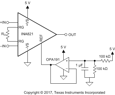
 Voltage reference devices are an excellent option for providing a low-impedance voltage source for the reference pin. However, if a resistor voltage divider generates a reference voltage, the divider must be buffered by an op amp, as Figure 67 shows, to avoid CMRR degradation.
 Figure 67. Using an Op Amp to Buffer Reference Voltages