ZHCSIM8C August   2018  – July 2019 INA821

PRODUCTION DATA.  

  1. 特性
  2. 应用
  3. 说明
    1.     Device Images
      1.      INA821 简化内部原理图
      2.      输入阶段失调电压漂移的典型分布
  4. 修订历史记录
  5. Device Comparison Table
  6. Pin Configuration and Functions
    1.     Pin Functions
  7. Specifications
    1. 7.1 Absolute Maximum Ratings
    2. 7.2 ESD Ratings
    3. 7.3 Recommended Operating Conditions
    4. 7.4 Thermal Information
    5. 7.5 Electrical Characteristics
    6. 7.6 Typical Characteristics: Table of Graphs
    7. 7.7 Typical Characteristics
  8. Detailed Description
    1. 8.1 Overview
    2. 8.2 Functional Block Diagram
    3. 8.3 Feature Description
      1. 8.3.1 Setting the Gain
        1. 8.3.1.1 Gain Drift
      2. 8.3.2 EMI Rejection
      3. 8.3.3 Input Common-Mode Range
      4. 8.3.4 Input Protection
      5. 8.3.5 Operating Voltage
      6. 8.3.6 Error Sources
    4. 8.4 Device Functional Modes
  9. Application and Implementation
    1. 9.1 Application Information
      1. 9.1.1 Reference Pin
      2. 9.1.2 Input Bias Current Return Path
    2. 9.2 Typical Application
      1. 9.2.1 Design Requirements
      2. 9.2.2 Detailed Design Procedure
      3. 9.2.3 Application Curves
    3. 9.3 Other Application Examples
      1. 9.3.1 Resistance Temperature Detector Interface
  10. 10Power Supply Recommendations
  11. 11Layout
    1. 11.1 Layout Guidelines
    2. 11.2 Layout Example
  12. 12器件和文档支持
    1. 12.1 器件支持
      1. 12.1.1 开发支持
    2. 12.2 文档支持
      1. 12.2.1 相关文档
    3. 12.3 接收文档更新通知
    4. 12.4 社区资源
    5. 12.5 商标
    6. 12.6 静电放电警告
    7. 12.7 Glossary
  13. 13机械、封装和可订购信息

封装选项

机械数据 (封装 | 引脚)
散热焊盘机械数据 (封装 | 引脚)
订购信息

Input Common-Mode Range

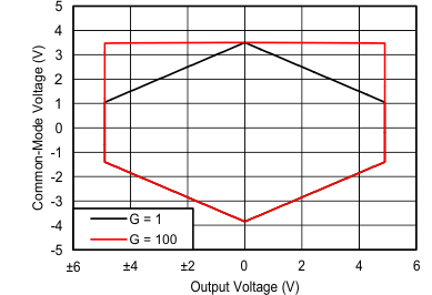
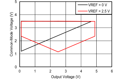
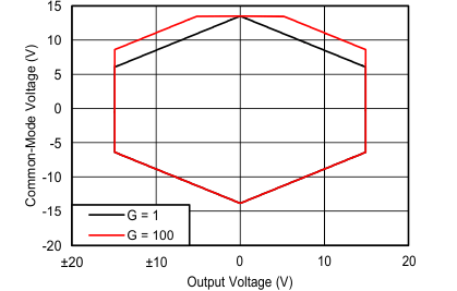
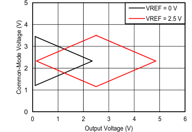
The linear input voltage range of the INA821 input circuitry extends within 2 V of power supplies and maintains excellent common-mode rejection throughout this range. The common-mode range for the most common operating conditions are shown in Figure 58 toFigure 61. The common-mode range for other operating conditions is best calculated using the Common-Mode Input Range Calculator for Instrumentation Amplifiers.
INA821 D054_SBOS959.gif
VS = 5 V G = 1
Figure 58. Input Common-Mode Voltage vs Output Voltage
INA821 D055_SBOS959.gif
VS = ±5 V VREF = 0 V
Figure 60. Input Common-Mode Voltage vs Output Voltage
INA821 D056_SBOS959.gif
VS = 5 V G = 100
Figure 59. Input Common-Mode Voltage vs Output Voltage
INA821 D052_SBOS959.gif
VS = ±15 V VREF = 0 V
Figure 61. Input Common-Mode Voltage vs Output Voltage