ZHCSIM8C August 2018 – July 2019 INA821
PRODUCTION DATA.
- 1 特性
- 2 应用
- 3 说明
- 4 修订历史记录
- 5 Device Comparison Table
- 6 Pin Configuration and Functions
- 7 Specifications
- 8 Detailed Description
- 9 Application and Implementation
- 10Power Supply Recommendations
- 11Layout
- 12器件和文档支持
- 13机械、封装和可订购信息
封装选项
机械数据 (封装 | 引脚)
散热焊盘机械数据 (封装 | 引脚)
- DRG|8
订购信息
8.3.1 Setting the Gain
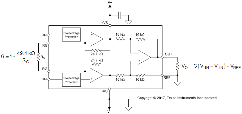
Figure 55 shows that the gain of the INA821 is set by a single external resistor (RG) connected between the RG pins (pins 1 and 8).
 Figure 55. Simplified Diagram of the INA821 With Gain and Output Equations
 The value of RG is selected according to:

Table 2 lists several commonly used gains and resistor values. The 49.4-kΩ term in Equation 1 is a result of the sum of the two internal 24.7-kΩ feedback resistors. These on-chip resistors are laser-trimmed to accurate absolute values. The accuracy and temperature coefficients of these resistors are included in the gain accuracy and drift specifications of the INA821. As shown in Figure 55 and explained in more details in the Layout section, make sure to connect low-ESR, 0.1-µF ceramic bypass capacitors between each supply pin and ground, that are placed as close to the device as possible.
Table 2. Commonly-Used Gains and Resistor Values
| DESIRED GAIN | RG (Ω) | NEAREST 1% RG (Ω) |
|---|---|---|
| 1 | NC | NC |
| 2 | 49.4 k | 49.9 k |
| 5 | 12.35 k | 12.4 k |
| 10 | 5.489 k | 5.49 k |
| 20 | 2.600 k | 2.61 k |
| 50 | 1.008 k | 1 k |
| 100 | 499 | 499 |
| 200 | 248 | 249 |
| 500 | 99 | 100 |
| 1000 | 49.4 | 49.9 |