ZHCSFO8C July 2016 – September 2023 INA250-Q1
PRODUCTION DATA
- 1
- 1 特性
- 2 应用
- 3 说明
- 4 Revision History
- 5 Pin Configuration and Functions
- 6 Specifications
- 7 Detailed Description
- 8 Applications and Implementation
- 9 Device and Documentation Support
- 10Mechanical, Packaging, and Orderable Information
7.3.1 Integrated Shunt Resistor
The INA250-Q1 features a precise, low-drift, current-sensing resistor to allow for precision measurements over the entire specified temperature range of –40°C to +125°C. The integrated current-sensing resistor ensures measurement stability overtemperature and improves layout and board constraint difficulties common in high precision measurements.
The onboard current-sensing resistor is designed as a 4-wire (or Kelvin) connected resistor that enables accurate measurements through a force-sense connection. Connecting the amplifier inputs pins (VIN– and VIN+) to the sense pins of the shunt resistor (SH– and SH+) eliminates many of the parasitic impedances commonly found in typical very-low sensing-resistor level measurements. Although the sense connection of the current-sensing resistor may be accessed through the SH+ and SH– pins, this resistor is not intended to be used as a stand-alone component. The INA250-Q1 device is system-calibrated to ensure that the current-sensing resistor and current-sensing amplifier are both precisely matched to one another. Using the shunt resistor without the onboard amplifier results in a current-sensing resistor tolerance of approximately 5%. To achieve the optimized system gain specification, the onboard sensing resistor must be used with the internal current-sensing amplifier.
The INA250-Q1 has approximately 4.5-mΩ of package resistance. 2 mΩ of this total package resistance is a precisely-controlled resistance from the Kelvin-connected current-sensing resistor used by the amplifier. The power dissipation requirements of the system and package are based on the total 4.5-mΩ package resistance between the IN+ and IN– pins. The heat dissipated across the package when current flows through the device ultimately determines the maximum current that may be safely handled by the package. The current consumption of the silicon is relatively low, leaving the total package resistance carrying the high load current as the primary contributor to the total power dissipation of the package. The maximum safe-operating current level ensures that the heat dissipated across the package is limited so that the resistor and the package are not damaged, and the internal junction temperature of the silicon does not exceed a +150°C limit.
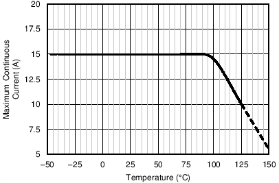
External factors (such as ambient temperature, external air flow, and PCB layout) may contribute to how effectively the heat developed from the current flowing through the total package resistance may be removed from the device. Under the conditions of no air flow, a maximum ambient temperature of +85°C, and 1-oz. copper input power planes, the INA250-Q1 device can accommodate continuous current levels up to 15 A. As shown in Figure 7-1, the current handling capability is derated at temperatures above the +85°C level with safe operation up to 10 A at a +125°C ambient temperature. With air flow and larger 2-oz. copper input power planes, the INA250-Q1 may safely accommodate continuous current levels up to 15 A over the entire –40°C to +125°C temperature range.
 Figure 7-1 Maximum Current vs Temperature