ZHCSFN6F March 2007 – June 2021 INA203 , INA204 , INA205
PRODUCTION DATA
- 1 特性
- 2 应用
- 3 说明
- 4 Revision History
- 5 Pin Configuration and Functions
-
6 Specifications
- 6.1 Absolute Maximum Ratings
- 6.2 ESD Ratings
- 6.3 Recommended Operating Conditions
- 6.4 Thermal Information
- 6.5 Electrical Characteristics: Current-Shunt Monitor
- 6.6 Electrical Characteristics: Comparator
- 6.7 Electrical Characteristics: Reference
- 6.8 Electrical Characteristics: General
- 6.9 Typical Characteristics
- 7 Detailed Description
- 8 Application and Implementation
- 9 Power Supply Recommendations
- 10Layout
- 11Device and Documentation Support
- 12Mechanical, Packaging, and Orderable Information
封装选项
请参考 PDF 数据表获取器件具体的封装图。
机械数据 (封装 | 引脚)
- D|14
- DGS|10
- PW|14
散热焊盘机械数据 (封装 | 引脚)
订购信息
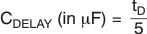
7.3.4 Comparator Delay (14-Pin Version Only)
The Comparator 2 programmable delay is controlled by a capacitor connected to the CMP2 Delay Pin; see Figure 7-3. The capacitor value (in μF) is selected by using Equation 1:
A simplified version of the delay circuit for Comparator 2 is shown in Figure 7-4. The delay comparator consists of two comparator stages with the delay between them. I1 and I2 cannot be turned on simultaneously; I1 corresponds to a U1 low output and I2 corresponds to a U1 high output. Using an initial assumption that the U1 output is low, I1 is on, then U2 +IN is zero. If U1 goes high, I2 supplies 120 nA to CDELAY. The voltage at U2 +IN begins to ramp toward a 0.6-V threshold. When the voltage crosses this threshold, the U2 output goes high while the voltage at U2 +IN continues to ramp up to a maximum of 1.2 V when given sufficient time (twice the value of the delay specified for CDELAY). This entire sequence is reversed when the comparator outputs go low, so that returning to low exhibits the same delay.
 Figure 7-4 Simplified Model of the Comparator 2 Delay Circuit
 Figure 7-5 Comparator Latching Capability
Take care to note what will happen if events occur more rapidly than the delay timeout; for example, when the U1 output goes high (turning on I2), but returns low (turning I1 back on) prior to reaching the 0.6-V transition for U2. The voltage at U2 +IN ramps back down at a rate determined by the value of CDELAY, and only returns to zero if given sufficient time.
In essence, when analyzing Comparator 2 for behavior with events more rapid than its delay setting, use the model shown in Figure 7-4.