ZHCSCL3 JUNE 2014 DS90UH925AQ-Q1
PRODUCTION DATA.
- 1 特性
- 2 应用范围
- 3 说明
- 4 简化电路原理图
- 5 修订历史记录
- 6 Pin Configuration and Functions
-
7 Specifications
- 7.1 Absolute Maximum Ratings
- 7.2 Handling Ratings
- 7.3 Recommended Operating Conditions
- 7.4 Thermal Information
- 7.5 DC Electrical Characteristics
- 7.6 AC Electrical Characteristics
- 7.7 Recommended Timing for the Serial Control Bus
- 7.8 DC and AC Serial Control Bus Characteristics
- 7.9 AC Timing Diagrams and Test Circuits
- 7.10 Switching Characteristics
- 7.11 Typical Characteristics
-
8 Detailed Description
- 8.1
Overview
- 8.1.1 Functional Block Diagram
- 8.1.2
Feature Description
- 8.1.2.1 High Speed Forward Channel Data Transfer
- 8.1.2.2 Low Speed Back Channel Data Transfer
- 8.1.2.3 Common Mode Filter Pin (CMF)
- 8.1.2.4 Video Control Signal Filter
- 8.1.2.5 Backward Compatible Mode
- 8.1.2.6 EMI Reduction Features
- 8.1.2.7 LVCMOS VDDIO Option
- 8.1.2.8 Power Down (PDB)
- 8.1.2.9 Remote Auto Power Down Mode
- 8.1.2.10 Input PCLK Loss Detect
- 8.1.2.11 Serial Link Fault Detect
- 8.1.2.12 Pixel Clock Edge Select (RFB)
- 8.1.2.13 Low Frequency Optimization (LFMODE)
- 8.1.2.14 Interrupt Pins - Funtional Description and Usage (INTB, REM_INTB)
- 8.1.2.15 GPIO[3:0] and GPO_REG[7:4]
- 8.1.2.16 I2S Transmitting
- 8.1.3 Built In Self Test (BIST)
- 8.1.4 Internal Pattern Generation
- 8.1.5 Change Summary from DS90UH925Q
- 8.2 Device Functional Modes
- 8.3 Programming
- 8.1
Overview
- 9 Application and Implementation
- 10Power Supply Recommendations
- 11Layout
- 12器件和文档支持
- 13机械封装和可订购信息
9 Application and Implementation
9.1 Application Information
The DS90UH925AQ, in conjunction with the DS90UH926Q, is intended for interface between a HDCP compliant host (graphics processor) and a Display. It supports a 24-bit color depth (RGB888) and high definition (720p) digital video format. It can receive a three 8-bit RGB stream with a pixel rate up to 85 MHz together with three control bits (VS, HS and DE) and three I2S-bus audio stream with an audio sampling rate up to 192 kHz. The included HDCP 1.3 compliant cipher block allows the authentication of the DS90UH926Q, which decrypts both video and audio contents. The keys are pre-loaded by TI into Non-Volatile Memory (NVM) for maximum security.
9.2 Typical Application
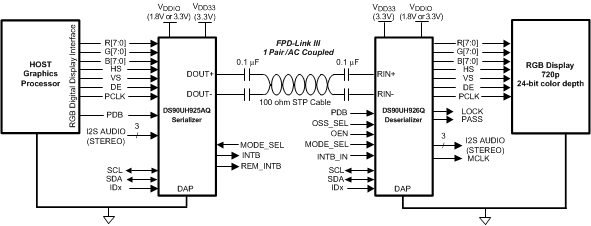 Figure 24. Typical Display System Diagram
9.2.1 Design Requirements
For the typical design application, use the following as input parameters.
Table 7. Design Parameters
| Design Parameter | Example Value |
|---|---|
| VDDIO | 1.8 V or 3.3 V |
| VDD33 | 3.3 V |
| AC Coupling Capacitor for DOUT± | 100 nF |
| PCLK Frequency | 85 MHz |
9.2.2 Detailed Design Procedure
9.2.2.1 Typical Application Connection
Figure 25 shows a typical application of the DS90UH925AQ serializer for an 85 MHz 24-bit Color Display Application. The CML outputs must have an external 0.1 μF AC coupling capacitor on the high speed serial lines. The serializer has an internal termination. Bypass capacitors are placed near the power supply pins. At a minimum, six (6) 4.7μF capacitors (and two (2) additional 1μF capacitors should be used for local device bypassing. Ferrite beads are placed on the two (2) VDDs (VDD33 and VDDIO) for effective noise suppression. The interface to the graphics source is with 3.3 V LVCMOS levels, thus the VDDIO pin is connected to the 3.3 V rail. A RC delay is placed on the PDB signal to delay the enabling of the device until power is stable.
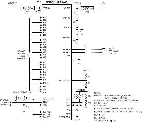 Figure 25. Typical Connection Diagram
9.2.2.2 Power Up Requirements and PDB Pin
When power is applied, the VDDIO supply needs to reach the expected operating voltage (1.8V or 3.3V) before the other supply (VDD33) begins to ramp. It is acceptable if both supplies ramp at the same time. The VDDs (VDD33 and VDDIO) supply ramp should be faster than 1.5 ms with a monotonic rise. A large capacitor on the PDB pin is needed to ensure PDB arrives after all the VDDs have settled to the recommended operating voltage. When PDB pin is pulled to VDDIO = 3.0 V to 3.6 V or VDD33, it is recommended to use a 10 kΩ pull-up and a >10 uF cap to GND to delay the PDB input signal.
All inputs must not be driven until VDD33 and VDDIO has reached its steady state value.
9.2.2.3 CML Interconnect Guidelines
See AN-1108 ( SNLA008) and AN-1187(SNLA035) for full details.
- Use 100 Ω coupled differential pairs
- Use the S/2S/3S rule in spacings
- S = space between the pair
- 2S = space between pairs
- 3S = space to LVCMOS signal
- Minimize the number of Vias
- Use differential connectors when operating above 500 Mbps line speed
- Maintain balance of the traces
- Minimize skew within the pair
Additional general guidance can be found in the LVDS Owner’s Manual - available in PDF format from the TI web site at: www.ti.com/lvds
9.2.2.4 Application Curves
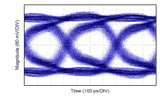 Figure 26. Serializer Eye Diagram at 2.73 Gbps Serial Data Rate
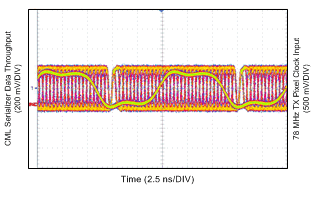 Figure 27. Serializer CML Output with 78MHz TX Pixel Clock