ZHCSCL3 JUNE 2014 DS90UH925AQ-Q1
PRODUCTION DATA.
- 1 特性
- 2 应用范围
- 3 说明
- 4 简化电路原理图
- 5 修订历史记录
- 6 Pin Configuration and Functions
-
7 Specifications
- 7.1 Absolute Maximum Ratings
- 7.2 Handling Ratings
- 7.3 Recommended Operating Conditions
- 7.4 Thermal Information
- 7.5 DC Electrical Characteristics
- 7.6 AC Electrical Characteristics
- 7.7 Recommended Timing for the Serial Control Bus
- 7.8 DC and AC Serial Control Bus Characteristics
- 7.9 AC Timing Diagrams and Test Circuits
- 7.10 Switching Characteristics
- 7.11 Typical Characteristics
-
8 Detailed Description
- 8.1
Overview
- 8.1.1 Functional Block Diagram
- 8.1.2
Feature Description
- 8.1.2.1 High Speed Forward Channel Data Transfer
- 8.1.2.2 Low Speed Back Channel Data Transfer
- 8.1.2.3 Common Mode Filter Pin (CMF)
- 8.1.2.4 Video Control Signal Filter
- 8.1.2.5 Backward Compatible Mode
- 8.1.2.6 EMI Reduction Features
- 8.1.2.7 LVCMOS VDDIO Option
- 8.1.2.8 Power Down (PDB)
- 8.1.2.9 Remote Auto Power Down Mode
- 8.1.2.10 Input PCLK Loss Detect
- 8.1.2.11 Serial Link Fault Detect
- 8.1.2.12 Pixel Clock Edge Select (RFB)
- 8.1.2.13 Low Frequency Optimization (LFMODE)
- 8.1.2.14 Interrupt Pins - Funtional Description and Usage (INTB, REM_INTB)
- 8.1.2.15 GPIO[3:0] and GPO_REG[7:4]
- 8.1.2.16 I2S Transmitting
- 8.1.3 Built In Self Test (BIST)
- 8.1.4 Internal Pattern Generation
- 8.1.5 Change Summary from DS90UH925Q
- 8.2 Device Functional Modes
- 8.3 Programming
- 8.1
Overview
- 9 Application and Implementation
- 10Power Supply Recommendations
- 11Layout
- 12器件和文档支持
- 13机械封装和可订购信息
7 Specifications
7.1 Absolute Maximum Ratings
over operating free-air temperature range (unless otherwise noted)(1)| PARAMETER | MIN | MAX | UNIT | ||
|---|---|---|---|---|---|
| VDD33 | Supply Voltage | –0.3 | +4.0 | V | |
| VDDIO | Supply Voltage | –0.3 | +4.0 | V | |
| LVCMOS I/O Voltage | –0.3 | VDDIO + 0.3 | V | ||
| Serializer Output Voltage | –0.3 | +2.75 | V | ||
| TJ | Junction Temperature | +150 | °C | ||
| For soldering specifications: see product folder at www.ti.com and www.ti.com/lit/an/snoa549c/snoa549c.pdf |
|||||
(1) Stresses beyond those listed under Absolute Maximum Ratings may cause permanent damage to the device. These are stress ratings only, which do not imply functional operation of the device at these or any other conditions beyond those indicated under Recommended Operating Conditions. Exposure to absolute-maximum-rated conditions for extended periods may affect device reliability.
7.2 Handling Ratings
| MIN | MAX | UNIT | ||||
|---|---|---|---|---|---|---|
| Tstg | Storage temperature range | 48 Lead WQFN Package | -65 | +150 | °C | |
| V(ESD) | Electrostatic discharge | Human body model (HBM), per AEC Q100-002(1) | -8 | +8 | kV | |
| Charged device model (CDM), per AEC Q100-011 | -1.25 | +1.25 | ||||
| Machine Model | -250 | +250 | V | |||
| ESD Rating (IEC 61000-4-2) RD = 330Ω, CS = 150pF |
Air Discharge (DOUT+, DOUT-) | -15 | +15 | kV | ||
| Contact Discharge (DOUT+, DOUT-) | -8 | +8 | ||||
| ESD Rating (ISO10605) RD = 330Ω, CS = 150pF RD = 2KΩ, CS = 150pF or 330pF |
Air Discharge (DOUT+, DOUT-) | -15 | +15 | kV | ||
| Contact Discharge (DOUT+, DOUT-) | -8 | +8 | ||||
(1) AEC Q100-002 indicates HBM stressing is done in accordance with the ANSI/ESDA/JEDEC JS-001 specification.
7.3 Recommended Operating Conditions
| MIN | TYP | MAX | UNIT | |
|---|---|---|---|---|
| Supply Voltage (VDD33) | 3.0 | 3.3 | 3.6 | V |
| LVCMOS Supply Voltage (VDDIO) | 3.0 | 3.3 | 3.6 | V |
| OR | ||||
| LVCMOS Supply Voltage (VDDIO) | 1.71 | 1.8 | 1.89 | V |
| Operating Free Air Temperature (TA) | −40 | +25 | +105 | °C |
| PCLK Frequency | 5 | 85 | MHz | |
| Supply Noise(6) | 100 | mVP-P | ||
7.4 Thermal Information
| THERMAL METRIC(1) | WQFN | UNIT | |
|---|---|---|---|
| 48 PINS | |||
| RθJA | Junction-to-ambient thermal resistance | 35 | °C/W |
| RθJC(top) | Junction-to-case (top) thermal resistance | 5.2 | |
| RθJB | Junction-to-board thermal resistance | 5.5 | |
| ψJT | Junction-to-top characterization parameter | 0.1 | |
| ψJB | Junction-to-board characterization parameter | 5.5 | |
| RθJC(bot) | Junction-to-case (bottom) thermal resistance | 1.3 | |
(1) For more information about traditional and new thermal metrics, see the IC Package Thermal Metrics application report, SPRA953.
7.5 DC Electrical Characteristics (1)(2)(3)
Over recommended operating supply and temperature ranges unless otherwise specified.| SYMBOL | PARAMETER | CONDITIONS | PIN/FREQ. | MIN | TYP | MAX | UNIT | |
|---|---|---|---|---|---|---|---|---|
| LVCMOS I/O DC SPECIFICATIONS | ||||||||
| VIH | High Level Input Voltage | VDDIO = 3.0 to 3.6 V | PDB | 2.0 | VDDIO | V | ||
| VIL | Low Level Input Voltage | VDDIO = 3.0 to 3.6 V | GND | 0.8 | V | |||
| IIN | Input Current | VIN = 0 V or VDDIO = 3.0 to 3.6 V | −10 | ±1 | +10 | μA | ||
| VIH | High Level Input Voltage | VDDIO = 3.0 to 3.6 V | R[7:0], G[7:0], B[7:0], HS, VS, DE, PCLK, I2S_CLK, I2S_WC, I2S_DA, I2S_DB | 2.0 | VDDIO | V | ||
| VDDIO = 1.71 to 1.89 V | 0.65* VDDIO |
VDDIO | V | |||||
| VIL | Low Level Input Voltage | VDDIO = 3.0 to 3.6 V | GND | 0.8 | V | |||
| VDDIO = 1.71 to 1.89 V | GND | 0.35* VDDIO |
V | |||||
| IIN | Input Current | VIN = 0 V or VDDIO | VDDIO = 3.0 to 3.6 V |
−10 | ±1 | +10 | μA | |
| VDDIO = 1.71 to 1.89 V |
−10 | ±1 | +10 | μA | ||||
| VOH | High Level Output Voltage | IOH = −4 mA | VDDIO = 3.0 to 3.6 V | GPIO[3:0], GPO_REG[7:4], REM_INTB | 2.4 | VDDIO | V | |
| VDDIO = 1.71 to 1.89 V |
VDDIO - 0.45 | VDDIO | V | |||||
| VOL | Low Level Output Voltage | IOL = +4 mA | VDDIO = 3.0 to 3.6 V | GND | 0.4 | V | ||
| VDDIO = 1.71 to 1.89 V |
GND | 0.35 | V | |||||
| IOS | Output Short Circuit Current | VOUT = 0 V | −50 | mA | ||||
| IOZ | TRI-STATE® Output Current | VOUT = 0 V or VDDIO, PDB = L, | −10 | +10 | μA | |||
| FPD-LINK III CML DRIVER DC SPECIFICATIONS | ||||||||
| VODp-p | Differential Output Voltage (DOUT+) – (DOUT-) |
RL = 100 Ω, Figure 1 | DOUT+, DOUT- | 1160 | 1250 | 1340 | mVp-p | |
| ΔVOD | Output Voltage Unbalance | 1 | 50 | mV | ||||
| VOS | Offset Voltage – Single-ended | RL = 100 Ω, Figure 1 | 2.5-0.25*VODp-p (TYP) | V | ||||
| ΔVOS | Offset Voltage Unbalance Single-ended |
1 | 50 | mV | ||||
| IOS | Output Short Circuit Current | DOUT+/- = 0 V, PDB = L or H |
−38 | mA | ||||
| RT | Internal Termination Resistor - Single ended | 40 | 52 | 62 | Ω | |||
| SUPPLY CURRENT | ||||||||
| IDD1 | Supply Current (includes load current) RL = 100 Ω, f = 85 MHz |
Checker Board Pattern, Figure 2 |
VDD33= 3.6 V | VDD33 | 148 | 170 | mA | |
| IDDIO1 | VDDIO = 3.6 V | VDDIO | 90 | 180 | μA | |||
| VDDIO = 1.89 V | 1 | 1.6 | mA | |||||
| IDDS1 | Supply Current Remote Auto Power Down Mode | 0x01[7] = 1, deserializer is powered down | VDD33 = 3.6 V | VDD33 | 1.2 | 2.4 | mA | |
| IDDIOS1 | VDDIO = 3.6 V | VDDIO | 65 | 150 | μA | |||
| VDDIO = 1.89 V | 55 | 150 | μA | |||||
| IDDS2 | Supply Current Power Down | PDB = L, All LVCMOS inputs are floating or tied to GND | VDD33 = 3.6 V | VDD33 | 1 | 2 | mA | |
| IDDIOS2 | VDDIO = 3.6 V | VDDIO | 65 | 150 | μA | |||
| VDDIO = 1.89 V | 50 | 150 | μA | |||||
7.6 AC Electrical Characteristics(1)(2)(3)
Over recommended operating supply and temperature ranges unless otherwise specified.| SYMBOL | PARAMETER | CONDITIONS | PIN/FREQ. | MIN | TYP | MAX | UNIT |
|---|---|---|---|---|---|---|---|
| GPIO BIT RATE | |||||||
| BR | Forward Channel Bit Rate | See(7)(8) | f = 5 – 85 MHz GPIO[3:0] |
0.25* f | Mbps | ||
| Back Channel Bit Rate | 75 | kbps | |||||
| RECOMMENDED TIMING FOR PCLK | |||||||
| tTCP | PCLK Period | See(7)(8) | PCLK | 11.76 | T | 200 | ns |
| tCIH | PCLK Input High Time | 0.4*T | 0.5*T | 0.6*T | ns | ||
| tCIL | PCLK Input Low Time | 0.4*T | 0.5*T | 0.6*T | ns | ||
| tCLKT | PCLK Input Transition Time Figure 3(7)(8) |
f = 5 MHz | 4.0 | ns | |||
| f = 85 MHz | 0.5 | ns | |||||
| tIJIT | PCLK Input Jitter Tolerance, Bit Error Rate ≤10-10 |
f / 40 < Jitter Freq < f / 20(7)(9) | f = 5 – 78 MHz | 0.4 | 0.6 | UI | |
7.7 Recommended Timing for the Serial Control Bus
Over 3.3 V supply and temperature ranges unless otherwise specified.| SYMBOL | PARAMETER | CONDITIONS | MIN | TYP | MAX | UNIT |
|---|---|---|---|---|---|---|
| fSCL | SCL Clock Frequency | Standard Mode | 0 | 100 | kHz | |
| Fast Mode | 0 | 400 | kHz | |||
| tLOW | SCL Low Period | Standard Mode | 4.7 | us | ||
| Fast Mode | 1.3 | us | ||||
| tHIGH | SCL High Period | Standard Mode | 4.0 | us | ||
| Fast Mode | 0.6 | us | ||||
| tHD;STA | Hold time for a start or a repeated start condition Figure 8 |
Standard Mode | 4.0 | us | ||
| Fast Mode | 0.6 | us | ||||
| tSU:STA | Set Up time for a start or a repeated start condition Figure 8 |
Standard Mode | 4.7 | us | ||
| Fast Mode | 0.6 | us | ||||
| tHD;DAT | Data Hold Time Figure 8 |
Standard Mode | 0 | 3.45 | us | |
| Fast Mode | 0 | 0.9 | us | |||
| tSU;DAT | Data Set Up Time Figure 8 |
Standard Mode | 250 | ns | ||
| Fast Mode | 100 | ns | ||||
| tSU;STO | Set Up Time for STOP Condition, Figure 8 | Standard Mode | 4.0 | us | ||
| Fast Mode | 0.6 | us | ||||
| tBUF | Bus Free Time Between STOP and START, Figure 8 |
Standard Mode | 4.7 | us | ||
| Fast Mode | 1.3 | us | ||||
| tr | SCL & SDA Rise Time, Figure 8 |
Standard Mode | 1000 | ns | ||
| Fast Mode | 300 | ns | ||||
| tf | SCL & SDA Fall Time, Figure 8 |
Standard Mode | 300 | ns | ||
| Fast mode | 300 | ns |
7.8 DC and AC Serial Control Bus Characteristics
Over 3.3 V supply and temperature ranges unless otherwise specified.(1)(2)(3)| SYMBOL | PARAMETER | CONDITIONS | MIN | TYP | MAX | UNIT |
|---|---|---|---|---|---|---|
| VIH | Input High Level | SDA and SCL | 0.7* VDD33 |
VDD33 | V | |
| VIL | Input Low Level Voltage | SDA and SCL | GND | 0.3* VDD33 |
V | |
| VHY | Input Hysteresis | >50 | mV | |||
| VOL | SDA, IOL = 1.25 mA | 0 | 0.36 | V | ||
| Iin | SDA or SCL, Vin = VDD33 or GND | -10 | +10 | µA | ||
| tR | SDA RiseTime – READ | SDA, RPU = 10 kΩ, Cb ≤ 400 pF, Figure 8 | 430 | ns | ||
| tF | SDA Fall Time – READ | 20 | ns | |||
| tSU;DAT | Set Up Time – READ | Figure 8 | 560 | ns | ||
| tHD;DAT | Hold Up Time – READ | Figure 8 | 615 | ns | ||
| tSP | Input Filter | 50 | ns | |||
| Cin | Input Capacitance | SDA or SCL | <5 | pF |
(1) The Electrical Characteristics tables list ensured specifications under the listed Recommended Operating Conditions except as otherwise modified or specified by the Electrical Characteristics Conditions and/or Notes. Typical specifications are estimations only and are not ensured.
(2) Typical values represent most likely parametric norms at VDD = 3.3 V, Ta = +25ºC, and at the Recommended Operation Conditions at the time of product characterization and are not ensured.
(3) Current into device pins is defined as positive. Current out of a device pin is defined as negative. Voltages are referenced to ground except VOD and ΔVOD, which are differential voltages.
(4) tPLD is the time required by the device to obtain lock when exiting power-down state with an active PCLK.
(5) UI – Unit Interval is equivalent to one serialized data bit width (1UI = 1/35*PCLK). The UI scales with PCLK frequency.
(6) Supply noise testing was done with minimum capacitors on the PCB. A sinusoidal signal is AC coupled to the VDD33 and VDDIOsupplies with amplitude = 100 mVp-p measured at the device VDD33 and VDDIO pins. Bit error rate testing of input to the Ser and output of the Des with 10 meter cable shows no error when the noise frequency on the Ser is less than 50 MHz. The Des on the other hand shows no error when the noise frequency is less than 50 MHz.
(7) Specification is ensured by characterization and is not tested in production.
(8) Specification is ensured by design and is not tested in production.
(9) Jitter Frequency is specified in conjunction with DS90UH926 PLL bandwidth.
7.9 AC Timing Diagrams and Test Circuits
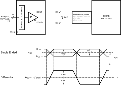
 Figure 1. Serializer VOD DC Output
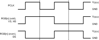
 Figure 2. Checkboard Data Pattern
 Figure 3. Serializer Input Clock Transition Time
 Figure 4. Serializer CML Output Load and Transition Time
 Figure 5. Serializer Setup and Hold Times
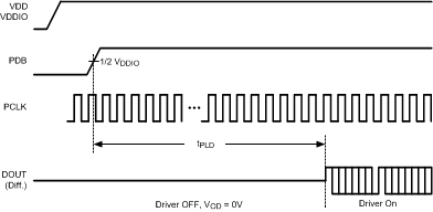
 Figure 6. Serializer Lock Time
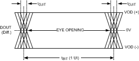
 Figure 7. Serializer CML Output Jitter
 Figure 8. Serial Control Bus Timing Diagram
7.10 Switching Characteristics
over operating free-air temperature range (unless otherwise noted)| SYMBOL | PARAMETER | TEST CONDITIONS | PIN/FREQ. | MIN | TYP | MAX | UNIT |
|---|---|---|---|---|---|---|---|
| tLHT | CML Output Low-to-High Transition Time | See Figure 4 | DOUT+, DOUT- | 80 | 130 | ps | |
| tHLT | CML Output High-to-Low Transition Time | 80 | 130 | ps | |||
| tDIS | Data Input Setup to PCLK | See Figure 5 | R[7:0], G[7:0], B[7:0], HS, VS, DE, PCLK, I2S_CLK, I2S_WC, I2S_DA | 2.0 | ns | ||
| tDIH | Data Input Hold from PCLK | 2.0 | ns | ||||
| tPLD | Serializer PLL Lock Time | Figure 6(4) | f = 15 - 45MHz | 131*T | ns | ||
| tSD | Delay — Latency | f = 15 - 45MHz | 145*T | ns | |||
| tTJIT | Output Total Jitter, Bit Error Rate ≥10-10 Figure 7(7)(8)(5) |
RL = 100Ω f = 45MHz |
DOUT+, DOUT- | 0.25 | 0.30 | UI |
7.11 Typical Characteristics

Note: On the rising edge of each clock period, the CML driver outputs a low Stop bit, high Start bit, and 33 DC-scrambled data bits.
Figure 9. Serializer CML Driver Output at 2.73 Gbps
 Figure 10. Comparison of Deserializer LVCMOS RX PCLK Output locked to a 78 MHz TX PCLK