ZHCSKE4C october 2016 – december 2020 DS280MB810
PRODUCTION DATA
- 1
- 1 特性
- 2 应用
- 3 说明
- 4 Revision History
- 5 Description (continued)
- 6 Pin Configuration and Functions
- 7 Specifications
- 8 Detailed Description
- 9 Application and Implementation
- 10Power Supply Recommendations
- 11Layout
- 12Device and Documentation Support
- 13Mechanical, Packaging, and Orderable Information
8.3.6 2x2 Cross-point Switch
Between each group of two adjacent channels (i.e. between channels 0–1, 2–3, 4–5, and 6–7) is a full 2x2 cross-point switch. The cross-point can be configured through pin-mode (shared register 0x05[1]=1) or SMBus registers (shared register 0x05[1]=0) to operate as follows:.
- Straight-thru mode
- Multiplex two inputs to one output
- Fanout one input to two outputs
- Cross two inputs to two outputs
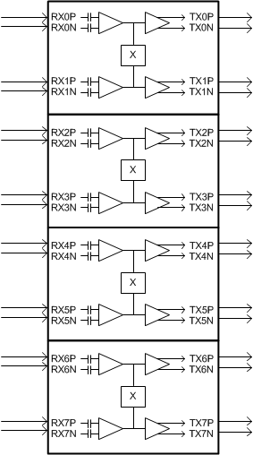
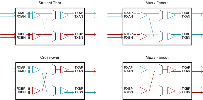
Figure 8-1 shows the four 2x2 cross-points available in the DS280MB810, and Figure 8-2 shows how each cross-point can be configured for straight-thru, multiplex, de-multiplex, or cross-over applications. Refer to the DS280MB810 Programming Guide for details on how to program the cross-point through SMBus registers.
 Figure 8-1 Block diagram showing all four 2x2 cross-points in the DS280MB810
 Figure 8-2 Signal distribution options available in each 2x2 cross-point (channel A can be 0, 2, 4, or 6; channel B can be 1, 3, 5, or 7)
The switching operation of the cross-point can be configured with the MUXSEL0 and MUXSEL1 pins when shared register 0x05[1]=1. Note that shared register 0x05[1] of both quads must be set to 1 to enable pin-control cross-point mode. Each quad can be selected through Reg_0xFF[5:4]. Refer to the DS280MB810 Programming Guide for more information.
The behavior of the cross-point (i.e. straight-thru, fanout, or mux) for each state of MUXSEL is illustrated in Figure 8-3. Note that MUXSEL0 controls channels 0, 1, 4, and 5; and MUXSEL1 controls channels 2, 3, 6, and 7.
 Figure 8-3 Signal distribution configuration options when using pin-control mode (channel A can be 0, 2, 4, or 6; channel B can be 1, 3, 5, or 7)