ZHCSG08E October 2016 – January 2021 DRV8702-Q1 , DRV8703-Q1
PRODUCTION DATA
- 1 特性
- 2 应用
- 3 说明
- 4 Revision History
- 5 Pin Configuration and Functions
- 6 Specifications
-
7 Detailed Description
- 7.1 Overview
- 7.2 Functional Block Diagram
- 7.3
Feature Description
- 7.3.1 Bridge Control
- 7.3.2 MODE Pin
- 7.3.3 nFAULT Pin
- 7.3.4 Current Regulation
- 7.3.5 Amplifier Output (SO)
- 7.3.6 PWM Motor Gate Drivers
- 7.3.7 IDRIVE Pin (DRV8702-Q1 Only)
- 7.3.8 Dead Time
- 7.3.9 Propagation Delay
- 7.3.10 Overcurrent VDS Monitor
- 7.3.11 VDS Pin (DRV8702-Q1 Only)
- 7.3.12 Charge Pump
- 7.3.13 Gate Drive Clamp
- 7.3.14
Protection Circuits
- 7.3.14.1 VM Undervoltage Lockout (UVLO2)
- 7.3.14.2 Logic Undervoltage (UVLO1)
- 7.3.14.3 VCP Undervoltage Lockout (CPUV)
- 7.3.14.4 Overcurrent Protection (OCP)
- 7.3.14.5 Gate Driver Fault (GDF)
- 7.3.14.6 Thermal Shutdown (TSD)
- 7.3.14.7 Watchdog Fault (WDFLT, DRV8703-Q1 Only)
- 7.3.14.8 Reverse Supply Protection
- 7.3.15 Hardware Interface
- 7.4 Device Functional Modes
- 7.5 Programming
- 7.6 Register Maps
- 8 Application and Implementation
- 9 Power Supply Recommendations
- 10Layout
- 11Device and Documentation Support
- 12Mechanical, Packaging, and Orderable Information
7.3.2 MODE Pin
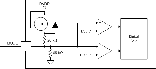
The MODE pin of the device determines the control interface and latches on power-up or when exiting sleep mode. #T4605616-36 shows an overview of the internal circuit of the MODE pin.
 Figure 7-4 MODE Pin Block Diagram
Table 7-6 lists the different control interfaces that can be set via MODE pin at power-up or when exiting sleep mode.
| MODE | CONTROL INTERFACE |
|---|---|
| 0 | PH or EN |
| 1 | Independent half-bridge |
| Hi-Z | PWM |
During the device power-up sequence, the DVDD pin is enabled first. Then the MODE pin latches. Finally the AVDD pin is enabled. For setting PWM control interface, TI does not recommended connecting the MODE pin to the AVDD pin. Instead the MODE pin should be connected to an external 5-V or 3.3-V supply or to the DVDD pin if not driven by an external microcontroller (MCU).