ZHCSG08E October 2016 – January 2021 DRV8702-Q1 , DRV8703-Q1
PRODUCTION DATA
- 1 特性
- 2 应用
- 3 说明
- 4 Revision History
- 5 Pin Configuration and Functions
- 6 Specifications
-
7 Detailed Description
- 7.1 Overview
- 7.2 Functional Block Diagram
- 7.3
Feature Description
- 7.3.1 Bridge Control
- 7.3.2 MODE Pin
- 7.3.3 nFAULT Pin
- 7.3.4 Current Regulation
- 7.3.5 Amplifier Output (SO)
- 7.3.6 PWM Motor Gate Drivers
- 7.3.7 IDRIVE Pin (DRV8702-Q1 Only)
- 7.3.8 Dead Time
- 7.3.9 Propagation Delay
- 7.3.10 Overcurrent VDS Monitor
- 7.3.11 VDS Pin (DRV8702-Q1 Only)
- 7.3.12 Charge Pump
- 7.3.13 Gate Drive Clamp
- 7.3.14
Protection Circuits
- 7.3.14.1 VM Undervoltage Lockout (UVLO2)
- 7.3.14.2 Logic Undervoltage (UVLO1)
- 7.3.14.3 VCP Undervoltage Lockout (CPUV)
- 7.3.14.4 Overcurrent Protection (OCP)
- 7.3.14.5 Gate Driver Fault (GDF)
- 7.3.14.6 Thermal Shutdown (TSD)
- 7.3.14.7 Watchdog Fault (WDFLT, DRV8703-Q1 Only)
- 7.3.14.8 Reverse Supply Protection
- 7.3.15 Hardware Interface
- 7.4 Device Functional Modes
- 7.5 Programming
- 7.6 Register Maps
- 8 Application and Implementation
- 9 Power Supply Recommendations
- 10Layout
- 11Device and Documentation Support
- 12Mechanical, Packaging, and Orderable Information
8.2.2.3 VDS Configuration
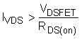
The VDS monitor threshold voltage, VDS(OCP), is configured based on the maximum current, IVDS, and RDS(on) of the FETs. The drain to source voltage, VDSFET, is the maximum current, IVDS, multiplied by the RDS(on) of the FET.
The VDS pin of the DRV8702-Q1 selects the VDS monitor trip threshold, VDS(OCP). The VDS bits in the VDS register of the DRV8703-Q1 selects the VDS(OCP) voltage. Use Equation 9 to calculate the trip current.
If the RDS(on) of the FET is 1.8 mΩ and the desired maximum current is less than 100 A, the VDSFET voltage is equal to 180 mV as shown in Equation 10.
For this example, select a value for the VDS(OCP) that is less than 180 mV. A VDS(OCP) value of 0.12 V was selected for this application.
To set the VDS(OCP) to 0.12 V, use the SPI (DRV8703-Q1 Only) or place a 33k resistor at the VDS pin to ground (DRV8702-Q1 Only).
The VDS pin can configured to select other VDS(OCP) threshold voltages. See the GUID-DD931F09-89B2-4344-A545-568F8A2BF37C.html#GUID-DD931F09-89B2-4344-A545-568F8A2BF37C section for more information on VDS operation.