ZHCSG08E October 2016 – January 2021 DRV8702-Q1 , DRV8703-Q1
PRODUCTION DATA
- 1 特性
- 2 应用
- 3 说明
- 4 Revision History
- 5 Pin Configuration and Functions
- 6 Specifications
-
7 Detailed Description
- 7.1 Overview
- 7.2 Functional Block Diagram
- 7.3
Feature Description
- 7.3.1 Bridge Control
- 7.3.2 MODE Pin
- 7.3.3 nFAULT Pin
- 7.3.4 Current Regulation
- 7.3.5 Amplifier Output (SO)
- 7.3.6 PWM Motor Gate Drivers
- 7.3.7 IDRIVE Pin (DRV8702-Q1 Only)
- 7.3.8 Dead Time
- 7.3.9 Propagation Delay
- 7.3.10 Overcurrent VDS Monitor
- 7.3.11 VDS Pin (DRV8702-Q1 Only)
- 7.3.12 Charge Pump
- 7.3.13 Gate Drive Clamp
- 7.3.14
Protection Circuits
- 7.3.14.1 VM Undervoltage Lockout (UVLO2)
- 7.3.14.2 Logic Undervoltage (UVLO1)
- 7.3.14.3 VCP Undervoltage Lockout (CPUV)
- 7.3.14.4 Overcurrent Protection (OCP)
- 7.3.14.5 Gate Driver Fault (GDF)
- 7.3.14.6 Thermal Shutdown (TSD)
- 7.3.14.7 Watchdog Fault (WDFLT, DRV8703-Q1 Only)
- 7.3.14.8 Reverse Supply Protection
- 7.3.15 Hardware Interface
- 7.4 Device Functional Modes
- 7.5 Programming
- 7.6 Register Maps
- 8 Application and Implementation
- 9 Power Supply Recommendations
- 10Layout
- 11Device and Documentation Support
- 12Mechanical, Packaging, and Orderable Information
7.5.1.2 SPI Format
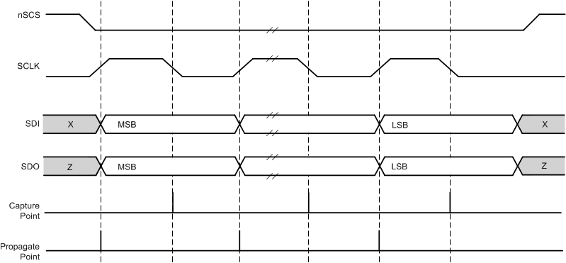
The SDI input-data word is 16 bits long and consists of the following format:
- 1 read or write bit, W (bit 15)
- 4 address bits, A (bits 14 through 11)
- 3 don't care bits, X (10 through 8)
- 8 data bits, D (7:0)
The SDO output-data word is 16 bits long and the first 8 bits are don’t care bits. The data word is the content of the register being accessed.
For a write command (W0 = 0), the response word on the SDO pin is the data currently in the register being written to.
For a read command (W0 = 1), the response word is the data currently in the register being read.
| R/W | ADDRESS | DON'T CARE | DATA | ||||||||||||
|---|---|---|---|---|---|---|---|---|---|---|---|---|---|---|---|
| B15 | B14 | B13 | B12 | B11 | B10 | B9 | B8 | B7 | B6 | B5 | B4 | B3 | B2 | B1 | B0 |
| W0 | A3 | A2 | A1 | A0 | X | X | X | D7 | D6 | D5 | D4 | D3 | D2 | D1 | D0 |
| DON'T CARE | DATA | ||||||||||||||
|---|---|---|---|---|---|---|---|---|---|---|---|---|---|---|---|
| B15 | B14 | B13 | B12 | B11 | B10 | B9 | B8 | B7 | B6 | B5 | B4 | B3 | B2 | B1 | B0 |
| X | X | X | X | X | X | X | X | D7 | D6 | D5 | D4 | D3 | D2 | D1 | D0 |
 Figure 7-18 SPI Transaction
The SCLK pin should be low at power-up of the device for reliable SPI transaction. If the SCLK pin cannot be guaranteed to be low at power-up, TI recommends performing a dummy SPI-read transaction (of any register) after power-up to ensure reliable subsequent transactions. Data read from this dummy read transaction should be discarded.