ZHCSMX4D September 2020 – March 2022 DRV8300
PRODUCTION DATA
- 1 特性
- 2 应用
- 3 说明
- 4 Revision History
- 5 Device Comparison Table
- 6 Pin Configuration and Functions
- 7 Specifications
- 8 Detailed Description
- 9 Application and Implementation
- 10Power Supply Recommendations
- 11Layout
- 12Device and Documentation Support
- 13Mechanical, Packaging, and Orderable Information
封装选项
机械数据 (封装 | 引脚)
散热焊盘机械数据 (封装 | 引脚)
- RGE|24
订购信息
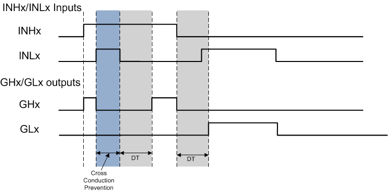
8.3.1.1.2 Deadtime and Cross-Conduction Prevention
In the DRV8300, high-side and low-side inputs operate independently, with an exception to prevent cross conduction when high and low side are turned ON at same time. The DRV8300 turns OFF high-side and low-side output to prevent shoot through when the both high-side and low-side inputs are at logic HIGH at same time.
The DRV8300 also provides option to insert additional deadtime to prevent the external high-side and low-side MOSFET from switching on at the same time. In the devices with DT pin (QFN package), deadtime can be linearly adjusted between 200 ns to 2000 ns by configuring resistor value between DT and GND. When the DT pin is left floating, fixed deadtime of 200 nS (typical value) is inserted. The value of resistor can be calculated using Equation 1.

In the devices without DT pin (TSSOP package), fixed deadtime of 200 ns (typical value) is inserted to prevent high and low side gate output turning ON at same time.
 Figure 8-3 Cross Conduction Prevention and
Deadtime Insertion