ZHCSOH4A July 2021 – August 2021 DLPC1438
PRODUCTION DATA
- 1 特性
- 2 应用
- 3 说明
- 4 Revision History
- 5 Pin Configuration and Functions
-
6 Specifications
- 6.1 Absolute Maximum Ratings
- 6.2 ESD Ratings
- 6.3 Recommended Operating Conditions
- 6.4 Thermal Information
- 6.5 Power Electrical Characteristics
- 6.6 Pin Electrical Characteristics
- 6.7 Internal Pullup and Pulldown Electrical Characteristics
- 6.8 DMD Sub-LVDS Interface Electrical Characteristics
- 6.9 DMD Low-Speed Interface Electrical Characteristics
- 6.10 System Oscillator Timing Requirements
- 6.11 Power Supply and Reset Timing Requirements
- 6.12 Parallel Interface Frame Timing Requirements
- 6.13 Parallel Interface General Timing Requirements
- 6.14 BT656 Interface General Timing Requirements
- 6.15 Flash Interface Timing Requirements
- 6.16 Other Timing Requirements
- 6.17 DMD Sub-LVDS Interface Switching Characteristics
- 6.18 DMD Parking Switching Characteristics
- 6.19 Chipset Component Usage Specification
- 7 Detailed Description
- 8 Application and Implementation
- 9 Power Supply Recommendations
- 10Layout
- 11Device and Documentation Support
- 12Mechanical, Packaging, and Orderable Information
11.1.2.1 Device Markings
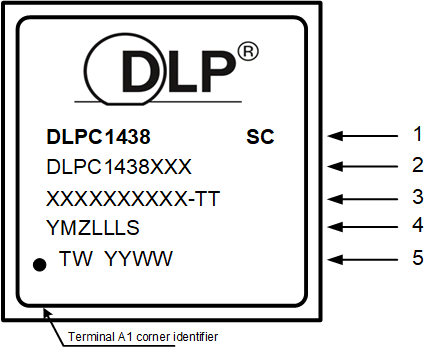
Marking Definitions:
| Line 1: | DLP® Device Name: DLPC1438 device name ID. SC: Solder ball composition e1: Indicates lead-free solder balls consisting of SnAgCu G8: G indicates mold compound green; 8 indicates lead-free solder balls consisting of tin-silver-copper (SnAgCu) with silver content less than or equal to 1.5% and that the mold compound meets TI's definition of green. |
| Line 2: | TI Part Number DLP® Device Name: DLPC1438 = x indicates 8 device name ID. XXX corresponds to the device package designator. |
| Line 3: | XXXXXXXXXX-TT Manufacturer part number |
| Line 4: | Foundry lot code for semiconductor wafers and lead-free solder ball marking YM: Year month date code Z: Site code LLL: Assembly lot code S: Site code May also be in the format LLLLLL.ZZZ LLLLLL: Fab lot number ZZZ: Lot split number |
| Line 5: | PH YYWW: Package assembly information PH: Manufacturing site YYWW: Date code (YY = Year :: WW = Week) |
Note:
- Engineering prototype samples are marked with an X suffix appended to the TI part number. For example, 2512737-0001X.