ZHCSK93 September 2019 DLP5534-Q1
ADVANCE INFORMATION for pre-production products; subject to change without notice.
- 1 特性
- 2 应用
- 3 说明
- 4 修订历史记录
- 5 Pin Configuration and Functions
-
6 Specifications
- 6.1 Absolute Maximum Ratings
- 6.2 Storage Conditions
- 6.3 ESD Ratings
- 6.4 Recommended Operating Conditions
- 6.5 Thermal Information
- 6.6 Electrical Characteristics
- 6.7 Timing Requirements
- 6.8 Switching Characteristics
- 6.9 System Mounting Interface Loads
- 6.10 Physical Characteristics of the Micromirror Array
- 6.11 Micromirror Array Optical Characteristics
- 6.12 Window Characteristics
- 6.13 Chipset Component Usage Specification
- 7 Detailed Description
- 8 Application and Implementation
- 9 Power Supply Recommendations
- 10Layout
- 11器件和文档支持
- 12机械、封装和可订购信息
7.5 Micromirror Array Temperature Calculation
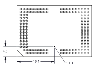
 Figure 19. DMD Thermal Test Points
 The active array temperature can be computed analytically from measurement points on the outside of the package, the package thermal resistance, the electrical power, and the illumination heat load.
Relationship between array temperature and the reference ceramic temperature (thermocouple location TP1 in Figure 19) is provided by the following equations:
where
- TARRAY = computed DMD array temperature (°C)
- TCERAMIC = measured ceramic temperature, TP1 location in Figure 19 (°C)
- RARRAY–TO–CERAMIC = DMD package thermal resistance from array to thermal test point TP1 (°C/W), see Thermal Information
- QARRAY = total power, electrical plus absorbed, on the DMD array (W)
- QELECTRICAL = nominal electrical power dissipation by the DMD (W)
- QINCIDENT = incident optical power to DMD (W)
- DMD Absorption Constant = 0.42
Electrical power dissipation of the DMD is variable and depends on the voltages, data rates, and operating frequencies.
Absorbed power from the illumination source is variable and depends on the operating state of the mirrors and the intensity of the light source.
Equations shown above are valid for a 1-chip DMD system with illumination distribution of 83.7% on the active array and 16.3% on the array border.
The following is a sample calculation for a typical projection application:
- QELECTRICAL = 0.4 W
- TCERAMIC = 55°C
- QINCIDENT = 3 W
- QARRAY = 0.4 W + (3 W × 0.42) = 1.66 W
- TARRAY = 55°C + (1.66 W × 1.1°C/W) = 56.8°C