ZHCSIG0G April 2016 – May 2019 DLP5531-Q1
PRODUCTION DATA.
- 1 特性
- 2 应用
- 3 说明
- 4 修订历史记录
- 5 Pin Configuration and Functions
-
6 Specifications
- 6.1 Absolute Maximum Ratings
- 6.2 Storage Conditions
- 6.3 ESD Ratings
- 6.4 Recommended Operating Conditions
- 6.5 Thermal Information
- 6.6 Electrical Characteristics
- 6.7 Timing Requirements
- 6.8 Switching Characteristics
- 6.9 System Mounting Interface Loads
- 6.10 Physical Characteristics of the Micromirror Array
- 6.11 Micromirror Array Optical Characteristics
- 6.12 Window Characteristics
- 6.13 Chipset Component Usage Specification
- 7 Detailed Description
- 8 Application and Implementation
- 9 Power Supply Recommendations
- 10Layout
- 11器件和文档支持
- 12机械、封装和可订购信息
7.6.1 Temperature Rise Through the Package for Heatsink Design
When designing the DMD heatsink solution, the package thermal resistance from array to reference ceramic temperature (thermocouple location TP1 in Figure 19) can be used to determine the temperature rise through the package as given by the following equations:
where
- TARRAY-TO-CERAMIC = temperature rise from array to thermal test point TP1 (°C/W)
- TCERAMIC = measured ceramic temperature, at the TP1 location in Figure 19 (°C)
- RARRAY–TO–CERAMIC = DMD package thermal resistance from array to thermal test point TP1 (°C/W)
See Thermal Information - QARRAY = total power, electrical plus absorbed, on the DMD array (W)
- QELECTRICAL = nominal electrical power dissipation by the DMD (W)
- QILLUMINATION = absorbed illumination heat load (W)
- QINCIDENT = incident power on the DMD (W)
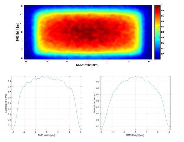
The DMD package thermal resistance from array to ceramic (RARRAY–TO–CERAMIC) assumes a non-uniform illumination distribution on the DMD as shown in Figure 20. For illumination profiles more uniform than the one highlighted in Figure 20, the value provided here is valid. However, for more non-uniform profiles (e.g. Gaussian distribution) the thermal resistance will be higher. Please contact TI to determine an accurate value for this case.
 Figure 20. Non-Uniform Illumination Profile
 The DMD absorption constant is a function of illumination distribution on the active array and the array border, angle of incidence (AOI), f number of the system, and operating state of the mirrors. The absorption constant is higher in the OFF state than in the ON state. Equations to calculate the absorption constant are provided for both ON and OFF mirror states. They assume an AOI of 34 degrees, an f/1.7 system, and they account for the distribution of light on the active array, POM, and array border.
Electrical power dissipation of the DMD is variable and depends on the voltages, data rates, and operating frequencies.
The following sample calculations assume 10% of the total incident light falls outside of the active array and POM, and the mirrors are in the OFF state.
- DMD Absorption Constant = 0.895 – 0.004783 × 90 = 0.46
- QELECTRICAL = 0.4 W
- RARRAY–TO–CERAMIC = 1.3°C/W
- QINCIDENT = 10 W
- QARRAY = 0.4 W + (0.46 × 10 W) = 5 W
- TARRAY-TO-CERAMIC = 5 W × 1.3°C/W = 6.5°C