ZHCSJA3B January   2019  – May 2022 DLP4500NIR

PRODUCTION DATA  

  1. 特性
  2. 应用范围
  3. 说明
  4. Revision History
  5. Chipset Component Usage Specification
  6. Pin Configuration and Functions
  7. Specifications
    1. 7.1  Absolute Maximum Ratings
    2. 7.2  Storage Conditions
    3. 7.3  ESD Ratings
    4. 7.4  Recommended Operating Conditions
    5. 7.5  Thermal Information
    6. 7.6  Electrical Characteristics
    7. 7.7  Timing Requirements
    8. 7.8  System Mounting Interface Loads
    9. 7.9  Micromirror Array Physical Characteristics
    10. 7.10 Micromirror Array Optical Characteristics
    11. 7.11 Typical Characteristics
  8. Detailed Description
    1. 8.1 Overview
    2. 8.2 Functional Block Diagram
    3. 8.3 Feature Description
    4. 8.4 Device Functional Modes
      1. 8.4.1 Operating Modes
    5. 8.5 Micromirror Array Temperature Calculation
      1. 8.5.1 Package Thermal Resistance
      2. 8.5.2 Case Temperature
        1. 8.5.2.1 Temperature Calculation
    6. 8.6 Micromirror Landed-on/Landed-Off Duty Cycle
      1. 8.6.1 Definition of Micromirror Landed-On/Landed-Off Duty Cycle
      2. 8.6.2 Landed Duty Cycle and Useful Life of the DMD
      3. 8.6.3 Landed Duty Cycle and Operational DMD Temperature
      4. 8.6.4 Estimating the Long-Term Average Landed Duty Cycle of a Product or Application
  9. Applications and Implementation
    1. 9.1 Application Information
    2. 9.2 Typical Application
      1. 9.2.1 Design Requirements
      2. 9.2.2 Detailed Design Procedure
        1. 9.2.2.1 DLPC350 System Interfaces
          1. 9.2.2.1.1 Control Interface
          2. 9.2.2.1.2 Input Data Interface
        2. 9.2.2.2 DLPC350 System Output Interfaces
          1. 9.2.2.2.1 Illumination Interface
          2. 9.2.2.2.2 Trigger Interface (Sync Outputs)
        3. 9.2.2.3 DLPC350 System Support Interfaces
          1. 9.2.2.3.1 Reference Clock
          2. 9.2.2.3.2 PLL
          3. 9.2.2.3.3 Program Memory Flash Interface
        4. 9.2.2.4 DMD Interfaces
          1. 9.2.2.4.1 DLPC350 to DMD Digital Data
          2. 9.2.2.4.2 DLPC350 to DMD Control Interface
          3. 9.2.2.4.3 DLPC350 to DMD Micromirror Reset Control Interface
  10. 10Power Supply Recommendations
    1. 10.1 Power Supply Sequencing Requirements
    2. 10.2 DMD Power Supply Power-Up Procedure
    3. 10.3 DMD Power Supply Power-Down Procedure
  11. 11Layout
    1. 11.1 Layout Guidelines
      1. 11.1.1 DMD Interface Design Considerations
      2. 11.1.2 DMD Termination Requirements
      3. 11.1.3 Decoupling Capacitors
      4. 11.1.4 Power Plane Recommendations
      5. 11.1.5 Signal Layer Recommendations
      6. 11.1.6 General Handling Guidelines for CMOS-Type Pins
      7. 11.1.7 PCB Manufacturing
        1. 11.1.7.1 General Guidelines
        2. 11.1.7.2 Trace Widths and Minimum Spacings
        3. 11.1.7.3 Routing Constraints
        4. 11.1.7.4 Fiducials
        5. 11.1.7.5 Flex Considerations
        6. 11.1.7.6 DLPC350 Thermal Considerations
    2. 11.2 Layout Example
      1. 11.2.1 Printed Circuit Board Layer Stackup Geometry
      2. 11.2.2 Recommended DLPC350 MOSC Crystal Oscillator Configuration
      3. 11.2.3 Recommended DLPC350 PLL Layout Configuration
  12. 12Device and Documentation Support
    1. 12.1 Device Support
      1. 12.1.1 第三方产品免责声明
      2. 12.1.2 Device Nomenclature
      3. 12.1.3 Device Markings
    2. 12.2 Documentation Support
      1. 12.2.1 Related Documentation
    3. 12.3 接收文档更新通知
    4. 12.4 支持资源
    5. 12.5 Trademarks
    6. 12.6 Electrostatic Discharge Caution
    7. 12.7 术语表
  13. 13Mechanical, Packaging, and Orderable Information

封装选项

机械数据 (封装 | 引脚)
散热焊盘机械数据 (封装 | 引脚)
订购信息

Recommended DLPC350 MOSC Crystal Oscillator Configuration

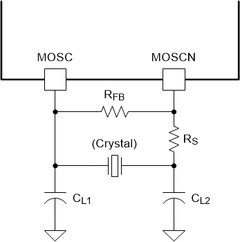
The DLPC350 controller requires an external reference clock to feed its internal PLL. This reference may be supplied via a crystal or oscillator. The DLPC350 controller accepts a reference clock of 32 MHz with a maximum frequency variation of 100 ppm (including aging, temperature, and trim component variation). When a crystal is used, several discrete components are also required, as shown in Figure 11-3.
GUID-5FD3171D-23C3-439C-9CBD-28082575A4CD-low.gif
CL = crystal load capacitance in F
CL1 = 2 × (CL – Cstray-MOSC)
CL2 = 2 × (CL – Cstray-MOSCN
Cstray-MOSC = sum of package and PCB capacitance at the crystal pin associated withe ASIC signal MOSC
Cstray-MOSCN = sum of package and PCB capacitance at the crystal pin associated withe ASIC signal MOSCN
Figure 11-3 Recommended Crystal Oscillator Configuration
Table 11-11 Crystal Port Electrical Characteristics
PARAMETERNOMUNIT
MOSC to GND capacitance3.9pF
MOSCN to GND capacitance3.8pF
Table 11-12 Recommended Crystal Configuration
PARAMETERRECOMMENDEDUNIT
Crystal circuit configurationParallel resonant
Crystal typeFundamental (first harmonic)
Crystal nominal frequency32MHz
Crystal frequency tolerance (including accuracy, temperature, aging and trim sensitivity)±100PPM
Crystal equivalent series resistance (ESR)50 maximumΩ
Crystal load10pF
Crystal shunt load7 maximumpF
Crystal frequency temperature stability±30PPM
RS drive resistor (nominal)100Ω
RFB feedback resistor (nominal)1
CL1 external crystal load capacitor (MOSC)Typical drive level with TCX9C3207001 crystal
(ESRmax = 30 Ω) = 160 µW. See Figure 11-3
pF
CL2 external crystal load capacitor (MOSCN)Typical drive level with TCX9C3207001 crystal
(ESRmax = 30 Ω) = 160 µW. See Figure 11-3
pF
PCB layoutA ground isolation ring around the crystal

If an external oscillator is used, then the oscillator output must drive the MOSC pin on the DLPC350 controller, and the MOSCN pin should be left unconnected. Note that the DLPC350 controller can only accept a triangular waveform.

Similar to the crystal option, the oscillator input frequency is limited to 32 MHz.

It is assumed that the external crystal or oscillator stabilizes within 50 ms after stable power is applied.