ZHCSPE1 February 2022 DLP3020-Q1
PRODUCTION DATA
- 1 特性
- 2 应用
- 3 说明
- 4 Revision History
- 5 Pin Configuration and Functions
-
6 Specifications
- 6.1 Absolute Maximum Ratings
- 6.2 Storage Conditions
- 6.3 ESD Ratings
- 6.4 Recommended Operating Conditions
- 6.5 Thermal Information
- 6.6 Electrical Characteristics
- 6.7 Timing Requirements
- 6.8 Switching Characteristics
- 6.9 System Mounting Interface Loads
- 6.10 Physical Characteristics of the Micromirror Array
- 6.11 Micromirror Array Optical Characteristics
- 6.12 Window Characteristics
- 6.13 Chipset Component Usage Specification
- 7 Detailed Description
- 8 Application and Implementation
- 9 Power Supply Recommendations
- 10Layout
- 11Device and Documentation Support
- 12Mechanical, Packaging, and Orderable Information
6.4 Recommended Operating Conditions
Over operating free-air temperature range (unless otherwise noted)
| MIN | NOM | MAX | UNIT | |||
|---|---|---|---|---|---|---|
| SUPPLY VOLTAGE RANGE | ||||||
| VREF | LVCMOS interface power supply voltage | 1.65 | 1.8 | 1.95 | V | |
| VCC | LVCMOS logic power supply voltage | 2.25 | 2.5 | 2.75 | V | |
| VOFFSET | Mirror electrode and HVCMOS voltage | 8.25 | 8.5 | 8.75 | V | |
| VBIAS | Mirror electrode voltage | 15.5 | 16 | 16.5 | V | |
| |VBIAS – VOFFSET| | Supply voltage delta (2) | 8.75 | V | |||
| VRESET | Mirror electrode voltage | –9.5 | –10 | –10.5 | V | |
| VP VT+ | Positive going threshold voltage | 0.4 × VREF | 0.7 × VREF | V | ||
| VN VT– | Negative going threshold voltage | 0.3 × VREF | 0.6 × VREF | V | ||
| VH ∆VT | Hysteresis voltage (Vp – Vn) | 0.1 × VREF | 0.4 × VREF | V | ||
| IOH_TDO | High level output current @ Voh = 2.25 V, TDO, Vcc = 2.25 V | –2 | mA | |||
| IOL_TDO | Low level output current @ Vol = 0.4 V, TDO, Vcc = 2.25 V | 2 | mA | |||
| TEMPERATURE DIODE | ||||||
| ITEMP_DIODE | Max current source into temperature diode (4) | 120 | µA | |||
| ENVIRONMENTAL | ||||||
| TARRAY(5) | Operating DMD array temperature - steady state (1) | –40 | 105 | °C | ||
| ILLUV(3) | Illumination, wavelength < 395 nm | 2.0 | mW/cm2 | |||
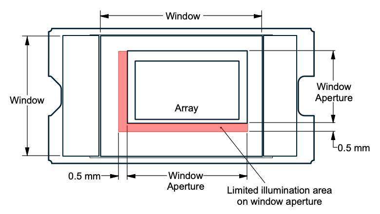
| ILLOVERFILL | Illumination overfill maximum heat load in area shown in Figure 6-1(6) | TARRAY ≤ 75°C | 26 | mW/mm2 | ||
| ILLOVERFILL | Illumination overfill maximum heat load in area shown in Figure 6-1(6) | TARRAY > 75°C | 20 | |||
(1) DMD active array temperature can be calculated as shown in Section 7.6 and assumes uniform illumination across the array.
(2) To prevent excess current, the supply voltage delta |VBIAS – VOFFSET| must be less than or equal to 8.75 V.
(3) The maximum operation conditions for DMD array temperature and illumination UV shall not be implemented simultaneously.
(4) Temperature diode is to assist in the calculation of the DMD array temperature during operation.
(5) Operating profile information for device micromirror landed duty-cycle and temperature may be provided if requested.
(6) The active area of the DLP3020-Q1 device is surrounded by an aperture on the inside of the DMD window surface that masks structures of the DMD device assembly from normal view. The aperture is sized to anticipate several optical conditions. Overfill light illuminating the area outside the active array can scatter and create adverse effects to the performance of an end application using the DMD. The illumination optical system should be designed to minimize light flux incident outside the active array. Depending on the particular system's optical architecture and assembly tolerances, the amount of overfill light on the outside of the active array may cause system performance degradation. Overfill illumination in excess of this specification may also impact thermal performance.
 Figure 6-1 Illumination Overfill Diagram