ZHCSJN3B March 2019 – May 2022 DLP2000
PRODUCTION DATA
- 1 特性
- 2 应用
- 3 说明
- 4 Revision History
- 5 Pin Configuration and Functions
-
6 Specifications
- 6.1 Absolute Maximum Ratings
- 6.2 Storage Conditions
- 6.3 ESD Ratings
- 6.4 Recommended Operating Conditions
- 6.5 Thermal Information
- 6.6 Electrical Characteristics
- 6.7 Timing Requirements
- 6.8 System Mounting Interface Loads
- 6.9 Physical Characteristics of the Micromirror Array
- 6.10 Micromirror Array Optical Characteristics
- 6.11 Window Characteristics
- 6.12 Chipset Component Usage Specification
- 7 Detailed Description
- 8 Application and Implementation
- 9 Power Supply Recommendations
- 10Layout
- 11Device and Documentation Support
- 12Mechanical, Packaging, and Orderable Information
9.2 Power Supply Power-Down Procedure
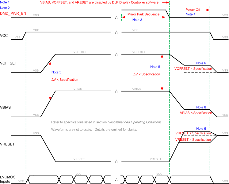
- The power-down sequence is the reverse order of the previous power-up sequence. VCC must be supplied until after VBIAS, VRESET and VOFFSET are discharged to within 4 V of ground.
- During Power-Down, it is not mandatory to stop driving VBIAS prior to VOFFSET, but it is a strict requirement that the delta between VBIAS and VOFFSET must be within ±8.75 V (Note 1).
- During power-down, the DMD’s LVCMOS input pins must be less than VCC + 0.3 V.
- During power-down, there is no requirement for the relative timing of VRESET with respect to VOFFSET and VBIAS.
- Slew rates for power-down are flexible, as long as the transient voltage levels follow the requirements listed previously.
 Figure 9-1 DMD Power Supply Sequencing Requirements
Note 1: Refer to specifications listed in Section 6.4. Waveforms are not to scale. Details are omitted for clarity.
Note 2: DMD_PWR_EN is not a package pin on the DMD. It is a signal from the DLP Display Controller (DLPC2607) that enables the VRESET, VBIAS, and VOFFSET regulators on the system board.
Note 3: After the DMD micromirror park sequence is complete, the DLP display controller (DLPC2607) software initiates a hardware power-down that disables VBIAS, VRESET and VOFFSET.
Note 4: During the micromirror parking process, VCC, VBIAS, VOFFSET, and VRESET power supplies are all required to be within the specification limits in Section 6.4. Once the micromirrors are parked, VBIAS, VOFFSET, and VRESET power supplies can be turned off.
Note 5: To prevent excess current, the supply voltage delta |VBIAS – VOFFSET| must be less than specified in Section 6.4. It is critical to meet this requirement and that VBIAS not reach full power level until after VOFFSET is at almost full power level. OEMs may find that the most reliable way to ensure this is to delay powering VBIAS until after VOFFSET is fully powered on during power-up (and to remove VBIAS prior to VOFFSET during power down). In this case, VOFFSET is run at its maximum allowable voltage level (8.75 V).
Note 6: Refer to specifications listed in Table 9-1.
| PARAMETER | DESCRIPTION | MIN | MAX | UNIT |
|---|---|---|---|---|
| VBIAS | Supply voltage level during power-down sequence | 4.0 | V | |
| VOFFSET | Supply voltage level during power-down sequence | 4.0 | V | |
| VRESET | Supply voltage level during power-down sequence | –4.0 | 0.5 | V |