ZHCSKJ2A November 2019 – April 2020 DAC60502 , DAC70502 , DAC80502
PRODUCTION DATA.
- 1 特性
- 2 应用
- 3 说明
- 4 修订历史记录
- 5 Device Comparison Table
- 6 Pin Configuration and Functions
-
7 Specifications
- 7.1 Absolute Maximum Ratings
- 7.2 ESD Ratings
- 7.3 Recommended Operating Conditions
- 7.4 Thermal Information
- 7.5 Electrical Characteristics
- 7.6 Timing Requirements : SPI Mode
- 7.7 Timing Requirements : I2C Standard Mode
- 7.8 Timing Requirements : I2C Fast Mode
- 7.9 Timing Requirements : I2C Fast-Mode Plus
- 7.10 Typical Characteristics
-
8 Detailed Description
- 8.1 Overview
- 8.2 Functional Block Diagram
- 8.3 Feature Description
- 8.4 Device Functional Modes
- 8.5 Programming
- 8.6
Register Maps
- 8.6.1
Registers
- 8.6.1.1 NOOP Register (offset = 0h) [reset = 0000h]
- 8.6.1.2 DEVID Register (offset = 1h) [reset = 0214h for DAC80502, 1214h for DAC70502, 2214h for DAC60502]
- 8.6.1.3 SYNC Register (offset = 2h) [reset = 0300h]
- 8.6.1.4 CONFIG Register (offset = 3h) [reset = 0000h]
- 8.6.1.5 GAIN Register (offset = 4h) [reset = 0003h]
- 8.6.1.6 TRIGGER Register (offset = 5h) [reset = 0000h]
- 8.6.1.7 BRDCAST Register (offset = 6h) [reset = 0000h for RSTSEL = 0, or reset = 8000h for RSTSEL = 1]
- 8.6.1.8 STATUS Register (offset = 7h) [reset = 0000h]
- 8.6.1.9 DAC-n Register (offset = 8h–9h) [reset = 0000h for RSTSEL = 0, or reset = 8000h for RSTSEL = 1]
- 8.6.1
Registers
- 9 Application and Implementation
- 10Power Supply Recommendations
- 11Layout
- 12器件和文档支持
- 13机械、封装和可订购信息
8.5.1.2 I2C Mode
The DACx0502 digital interface is programmed to work in I2C mode when the logic level of the SPI2C pin is 1 at power up. In I2C mode, the DACx0502 have a 2-wire serial interface: SCL, SDA, and one address pin, A0. The I2C bus consists of a data line (SDA) and a clock line (SCL) with pull-up structures. When the bus is idle, both the SDA and SCL lines are pulled high. All the I2C-compatible devices connect to the I2C bus through open-drain I/O pins SDA and SCL.
The I2C specification states that the device that controls communication is called a master, and the devices that are controlled by the master are called slaves. The master device generates the SCL signal. The master device also generates special timing conditions (start condition, repeated start condition, and stop condition) on the bus to indicate the start or stop of a data transfer. Device addressing is completed by the master. The master device on an I2C bus is typically a microcontroller or DSP. The DACx0502 operate as a slave device on the I2C bus. A slave device acknowledges master commands, and upon master control, receives or transmits data.
Typically, the DACx0502 operate as a slave receiver. A master device writes to the DACx0502, a slave receiver. However, if a master device requires the DACx0502 internal register data, the DACx0502 operate as a slave transmitter. In this case, the master device reads from the DACx0502 According to I2C terminology, read and write refer to the master device.
The DACx0502 are slave devices that support the following data transfer modes:
- Standard mode (100 kbps)
- Fast mode (400 kbps)
- Fast-mode plus (1.0 Mbps)
The data transfer protocol for standard and fast modes is exactly the same; therefore, these modes are referred to as F/S-mode in this document. The fast-mode plus protocol is supported in terms of data transfer speed, but not output current. The low-level output current would be 3 mA, similar to the case of standard and fast modes. The DACx0502 support 7-bit addressing. The 10-bit addressing mode is not supported. These devices support the general call reset function. Sending the following sequence initiates a software reset within the device: start/repeated start, 0x00, 0x06, stop. The reset is asserted within the device on the falling edge of the ACK bit, following the second byte.
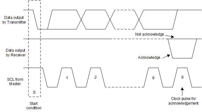
Other than specific timing signals, the I2C interface works with serial bytes. At the end of each byte, a ninth clock cycle generates and detects an acknowledge signal. Acknowledge is when the SDA line is pulled low during the high period of the ninth clock cycle. A not-acknowledge is when the SDA line is left high during the high period of the ninth clock cycle as shown in Figure 59.
 Figure 59. Acknowledge and Not Acknowledge on the I2C Bus