ZHCSO96B June 2021 – June 2022 DAC12DL3200
PRODUCTION DATA
- 1 特性
- 2 应用
- 3 说明
- 4 Revision History
- 5 Pin Configuration and Functions
-
6 Specifications
- 6.1 Absolute Maximum Ratings
- 6.2 ESD Ratings
- 6.3 Recommended Operating Conditions
- 6.4 Thermal Information
- 6.5 Electrical Characteristics - DC Specifications
- 6.6 Electrical Characteristics - Power Consumption
- 6.7 Electrical Characteristics - AC Specifications
- 6.8 Timing Requirements
- 6.9 Switching Characteristics
- 6.10 Typical Characteristics
-
7 Detailed Description
- 7.1 Overview
- 7.2 Functional Block Diagram
- 7.3
Feature Description
- 7.3.1 DAC Output Modes
- 7.3.2 DAC Output Interface
- 7.3.3 LVDS Interface
- 7.3.4 Multi-Device Synchronization (SYSREF+/-)
- 7.3.5 Alarms
- 7.4 Device Functional Modes
- 7.5 Programming
- 8 Application and Implementation
- 9 Device and Documentation Support
- 10Mechanical, Packaging, and Orderable Information
封装选项
机械数据 (封装 | 引脚)
散热焊盘机械数据 (封装 | 引脚)
订购信息
7.3.2.3 Example Analog Output Interfaces
There are numerous ways to interface with the DAC analog output. A few are shown below. In all cases a DC path for current must be provided from a positive voltage source, typically VADAC18+. Further, the voltage at each output pin must be within the compliance voltage range for all digital codes.
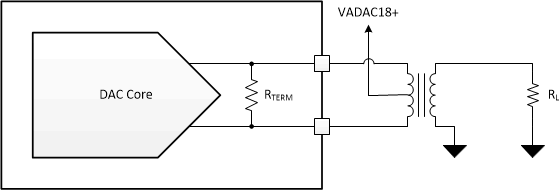
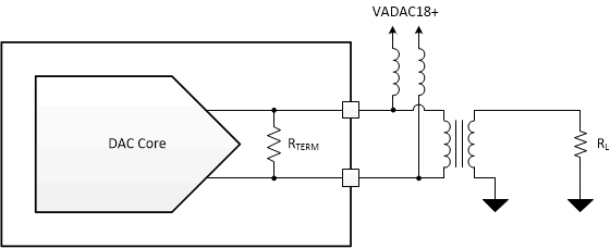
The most common interface makes use of a transformer or balun. Some transformers have a center tap that can be used to provide a DC bias to the secondary transformer winding. This is demonstrated in Figure 7-10. For a center-tapped transformer the center tap should be tied to the VDDA18A and VDDA18B supply voltages. RF choke inductors can be used to provide the DC bias for baluns without a center tap as shown in Figure 7-11. The chokes should be well matched and carefully laid out in order to optimize even order distortion suppression. Many high frequency baluns will not have a center tap for the DC bias.
 Figure 7-10 DAC Output Interface using Center-Tapped Transformer
 Figure 7-11 DAC Output Interface using RF Chokes and Transformer
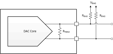
Both transformer and balun output interfaces will not pass DC and low frequency signals. Instead, a higher bias voltage should be used with pull-up resistors to bias the DAC within its compliance voltage range. Careful supply sequencing is required to prevent damage to the DAC if VBIAS exceeds the absolute maximum rated voltage. In all cases, voltages at the DAC pins must be within the absolute maximum rated voltages.
 Figure 7-12 DAC Output Interface with DC Coupling