ZHCSEW3C April   2016  – February 2022 CSD17382F4

PRODUCTION DATA  

  1. 1特性
  2. 2应用
  3. 3说明
  4. 4Revision History
  5. 5Specifications
    1. 5.1 Electrical Characteristics
    2. 5.2 Thermal Information
    3. 5.3 Typical MOSFET Characteristics
  6. 6Device and Documentation Support
    1. 6.1 支持资源
    2. 6.2 Receiving Notification of Documentation Updates
    3. 6.3 Trademarks
    4. 6.4 Electrostatic Discharge Caution
    5. 6.5 术语表
  7. 7Mechanical, Packaging, and Orderable Information
    1. 7.1 Mechanical Dimensions
    2. 7.2 Recommended Minimum PCB Layout
    3. 7.3 Recommended Stencil Pattern
    4. 7.4 CSD17382F4 Embossed Carrier Tape Dimensions

封装选项

请参考 PDF 数据表获取器件具体的封装图。

机械数据 (封装 | 引脚)
  • YJC|3
散热焊盘机械数据 (封装 | 引脚)
订购信息

Mechanical Dimensions

GUID-20220106-SS0I-JSBJ-G13J-2NLDBJ0DSBCT-low.gif
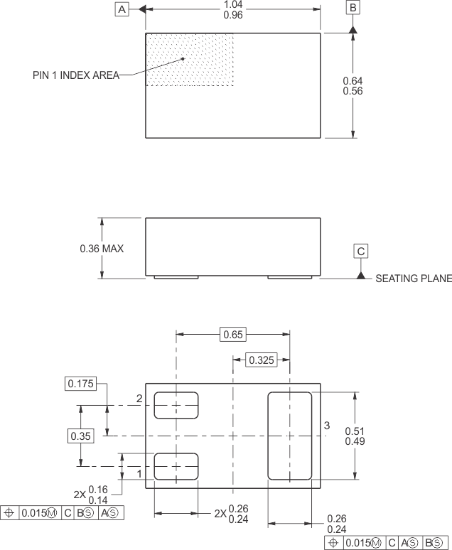
All linear dimensions are in millimeters. Any dimensions in parenthesis are for reference only. Dimensioning and tolerancing per ASME Y14.5M.
This drawing is subject to change without notice.
This package is a Pb-free bump design. Bump finish may vary. To determine the exact finish, refer to the device datasheet or contact a local TI representative.