ZHCSJU4I November 2006 – September 2018 CC1020
PRODUCTION DATA.
- 1器件概述
- 2修订历史记录
- 3Terminal Configuration and Functions
-
4Specifications
- 4.1 Absolute Maximum Ratings
- 4.2 ESD Ratings
- 4.3 Recommended Operating Conditions
- 4.4 RF Transmit
- 4.5 RF Receive
- 4.6 RSSI / Carrier Sense
- 4.7 Intermediate Frequency (IF)
- 4.8 Crystal Oscillator
- 4.9 Frequency Synthesizer
- 4.10 Digital Inputs and Outputs
- 4.11 Current Consumption
- 4.12 Thermal Resistance Characteristics for VQFNP Package
-
5Detailed Description
- 5.1 Overview
- 5.2 Functional Block Diagram
- 5.3 Configuration Overview
- 5.4 Microcontroller Interface
- 5.5 4-wire Serial Configuration Interface
- 5.6 Signal Interface
- 5.7 Data Rate Programming
- 5.8 Frequency Programming
- 5.9
Receiver
- 5.9.1 IF Frequency
- 5.9.2 Receiver Channel Filter Bandwidth
- 5.9.3 Demodulator, Bit Synchronizer, and Data Decision
- 5.9.4 Receiver Sensitivity Versus Data Rate and Frequency Separation
- 5.9.5 RSSI
- 5.9.6 Image Rejection Calibration
- 5.9.7 Blocking and Selectivity
- 5.9.8 Linear IF Chain and AGC Settings
- 5.9.9 AGC Settling
- 5.9.10 Preamble Length and Sync Word
- 5.9.11 Carrier Sense
- 5.9.12 Automatic Power-up Sequencing
- 5.9.13 Automatic Frequency Control
- 5.9.14 Digital FM
- 5.10 Transmitter
- 5.11 Input and Output Matching and Filtering
- 5.12 Frequency Synthesizer
- 5.13 VCO and LNA Current Control
- 5.14 Power Management
- 5.15 On-Off Keying (OOK)
- 5.16 Crystal Oscillator
- 5.17 Built-in Test Pattern Generator
- 5.18 Interrupt on Pin DCLK
- 5.19 PA_EN and LNA_EN Digital Output Pins
- 5.20 System Considerations and Guidelines
- 5.21 Antenna Considerations
- 5.22 Configuration Registers
- 6Applications, Implementation, and Layout
- 7器件和文档支持
- 8机械、封装和可订购信息
5.9.12 Automatic Power-up Sequencing
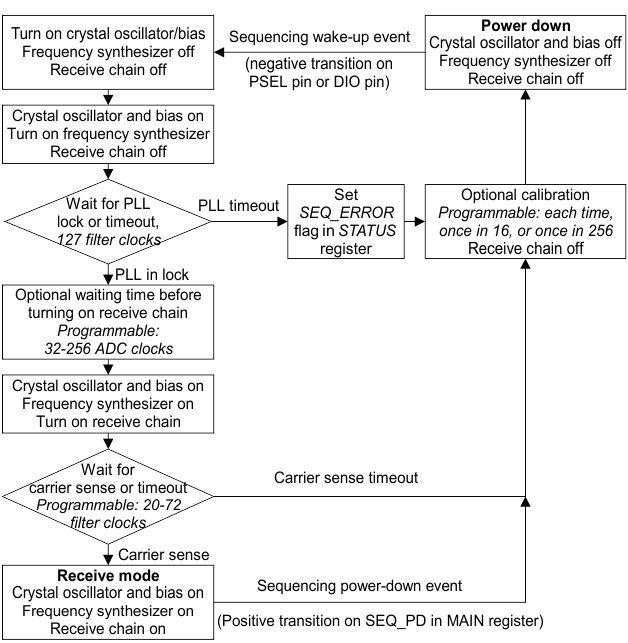
The CC1020 device has a built-in automatic power-up sequencing state machine. By setting the CC1020 device into this mode, the receiver can be powered-up automatically by a wake-up signal and will then check for a carrier signal (carrier sense). If carrier sense is not detected, it returns to power-down mode. A flow chart for automatic power-up sequencing is shown in Figure 5-16.
The automatic power-up sequencing mode is selected when PD_MODE[1:0] = 11 in the MAIN register. When the automatic power-up sequencing mode is selected, the functionality of the MAIN register is changed and used to control the sequencing.
By setting SEQ_PD = 1 in the MAIN register, the CC1020 device is set in power down mode. If SEQ_PSEL = 1 in the SEQUENCING register the automatic power-up sequence is initiated by a negative transition on the PSEL pin.
If SEQ_PSEL = 0 in the SEQUENCING register, then the automatic power-up sequence is initiated by a negative transition on the DIO pin (as long as SEP_DI_DO = 1 in the INTERFACE register).
Sequence timing is controlled through RX_WAIT[2:0] AND CS_WAIT[3:0] in the SEQUENCING register.
VCO and PLL calibration can also be done automatically as a part of the sequence. This is controlled through SEQ_CAL[1:0] in the MAIN register. Calibration can be done every time, every 16th sequence, every 256th sequence, or never. See Section 5.22.1 description for details. A description of when to do, and how the VCO and PLL self-calibration is done, is given in Section 5.12.2.
See also Application Note AN070 CC1020 Automatic Power-Up Sequencing (SWRA279).

 where ADC_DIV[2:0] is set in the MODEM register.