ZHCSJU4I November 2006 – September 2018 CC1020
PRODUCTION DATA.
- 1器件概述
- 2修订历史记录
- 3Terminal Configuration and Functions
-
4Specifications
- 4.1 Absolute Maximum Ratings
- 4.2 ESD Ratings
- 4.3 Recommended Operating Conditions
- 4.4 RF Transmit
- 4.5 RF Receive
- 4.6 RSSI / Carrier Sense
- 4.7 Intermediate Frequency (IF)
- 4.8 Crystal Oscillator
- 4.9 Frequency Synthesizer
- 4.10 Digital Inputs and Outputs
- 4.11 Current Consumption
- 4.12 Thermal Resistance Characteristics for VQFNP Package
-
5Detailed Description
- 5.1 Overview
- 5.2 Functional Block Diagram
- 5.3 Configuration Overview
- 5.4 Microcontroller Interface
- 5.5 4-wire Serial Configuration Interface
- 5.6 Signal Interface
- 5.7 Data Rate Programming
- 5.8 Frequency Programming
- 5.9
Receiver
- 5.9.1 IF Frequency
- 5.9.2 Receiver Channel Filter Bandwidth
- 5.9.3 Demodulator, Bit Synchronizer, and Data Decision
- 5.9.4 Receiver Sensitivity Versus Data Rate and Frequency Separation
- 5.9.5 RSSI
- 5.9.6 Image Rejection Calibration
- 5.9.7 Blocking and Selectivity
- 5.9.8 Linear IF Chain and AGC Settings
- 5.9.9 AGC Settling
- 5.9.10 Preamble Length and Sync Word
- 5.9.11 Carrier Sense
- 5.9.12 Automatic Power-up Sequencing
- 5.9.13 Automatic Frequency Control
- 5.9.14 Digital FM
- 5.10 Transmitter
- 5.11 Input and Output Matching and Filtering
- 5.12 Frequency Synthesizer
- 5.13 VCO and LNA Current Control
- 5.14 Power Management
- 5.15 On-Off Keying (OOK)
- 5.16 Crystal Oscillator
- 5.17 Built-in Test Pattern Generator
- 5.18 Interrupt on Pin DCLK
- 5.19 PA_EN and LNA_EN Digital Output Pins
- 5.20 System Considerations and Guidelines
- 5.21 Antenna Considerations
- 5.22 Configuration Registers
- 6Applications, Implementation, and Layout
- 7器件和文档支持
- 8机械、封装和可订购信息
5.9.5 RSSI
The CC1020 device has a built-in RSSI (Received Signal Strength Indicator) giving a digital value that can be read form the RSSI register. The RSSI reading must be offset and adjusted for VGA gain setting (VGA_SETTING[4:0] in the VGA3 register).
The digital RSSI value is ranging from 0 to 106 (7 bits).
The RSSI reading is a logarithmic measure of the average voltage amplitude after the digital filter in the digital part of the IF chain as shown in Equation 18.
The relative power is then given by RSSI × 1.5 dB in a logarithmic scale.
The number of samples used to calculate the average signal amplitude is controlled by AGC_AVG[1:0] in the VGA2 register. The RSSI update rate is given by Equation 19.

Where:
AGC_AVG[1:0] is set in the VGA2 register.
ffilter_clock = 2 × ChBW.
Maximum VGA gain is programmed by the VGA_SETTING[4:0] bits. The VGA gain is programmed in approximately 3 dB/LSB. The RSSI measurement can be referred to the power (absolute value) at the RF_IN pin by using the Equation 20.
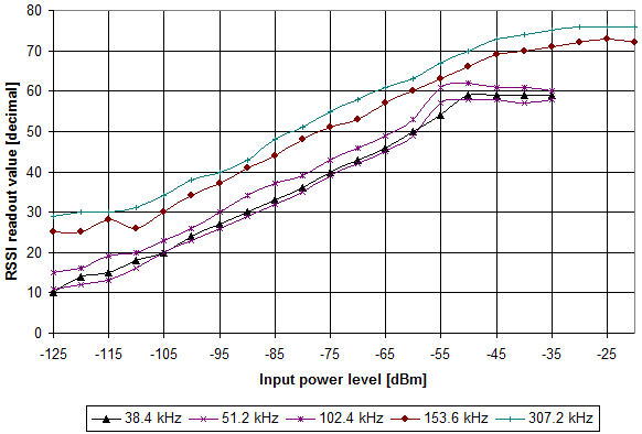
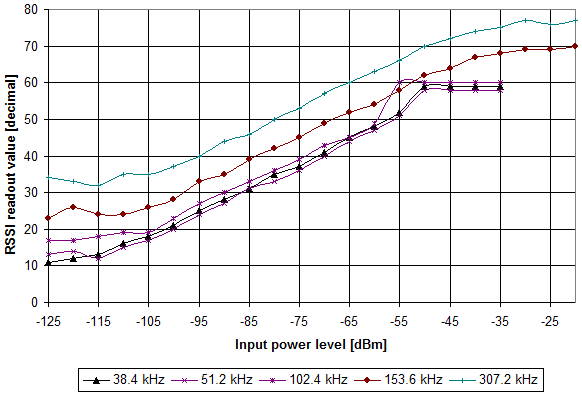
The RSSI_Offset depends on the channel filter bandwidth used due to different VGA settings. Figure 5-11 and Figure 5-12 show typical plots of RSSI reading as a function of input power for different channel spacings. See Section 5.9.5 for a list of channel filter bandwidths corresponding to the various channel spacings. Refer to AN030 CC1020/1021 Received Signal Strength Indicator (SWRA062) for further details.
The method shown in Equation 21 can be used to calculate the power (P) in dBm from the RSSI readout values in Figure 5-11 and Figure 5-12.
Where:
P is the output power in dBm for the current RSSI readout value.
RSSI_ref is the RSSI readout value taken from Figure 5-11 or Figure 5-12 for an input power level of P_ref.
NOTE
The RSSI reading in decimal value changes for different channel filter bandwidths.
The analog filter has a finite dynamic range and is the reason why the RSSI reading is saturated at lower channel spacings. Higher channel spacing is typically used for high frequency deviation and data rates. The analog filter bandwidth is about 160 kHz and is bypassed for high frequency deviation and data rates and is the reason why the RSSI reading is not saturated for 200 kHz and 500 kHz channel spacing in Figure 5-11 and Figure 5-12.

