ZHCSCF9 May 2014 BUF16821-Q1
PRODUCTION DATA.
- 1 特性
- 2 应用范围
- 3 说明
- 4 修订历史记录
- 5 Pin Configuration and Functions
- 6 Specifications
-
7 Detailed Description
- 7.1 Overview
- 7.2 Functional Block Diagram
- 7.3 Feature Description
- 7.4 Device Functional Modes
- 7.5 Programming
- 7.6 Register Maps
- 8 Application and Implementation
- 9 Power Supply Recommendations
- 10Layout
- 11器件和文档支持
- 12机械封装和可订购信息
8 Application and Implementation
8.1 Application Information
The BUF16821-Q1 is a multichannel programmable voltage reference. Featuring 16 programmable gamma reference outputs and two programmable VCOM outputs, the device is designed to interface between timing controllers and source drivers commonly used in LCD displays.
8.2 Typical Application
 Figure 20. Gamma Control Block Diagram
8.2.1 Design Requirements
If the nonvolatile memory has never been programmed, the BUF16821-Q1 outputs defaults to VS / 2 following power-up. Refer to the Power Supply Recommendations section for proper power-supply sequencing requirements. Figure 21 shows the typical output response when the analog power supply (VS) ramps to its desired value. When the analog supply is below 2 V, the outputs follow the analog supply voltage. After the analog supply voltage (VS) exceeds approximately 2 V, the outputs begin to track at VS / 2. This sequence is illustrated in Figure 21.
If the nonvolatile memory is pre-programmed, the device outputs ramp to their pre-programmed values. Figure 22 and Figure 23 illustrate the power-up behavior of the device pre-programmed to a 4-V and 8-V output voltage, respectively. Note that when the analog power supply voltage (VS) exceeds approximately 5 V, the device performs an automatic read of the nonvolatile memory, acquiring the pre-programmed values to ensure the proper output value when the analog supply voltage ramps to its final value. During the nonvolatile memory acquire operation, the output tracks at VS / 2 for approximately 1 ms. This sequence is illustrated in Figure 22 and Figure 23 . Note that the minimum valid analog supply voltage, VS, is specified as 9 V. Below this value the outputs should not be considered valid.
Figure 24 illustrates the device output response to a general-call reset. During the internal reset, the output momentarily tracks at VS / 2 while the nonvolatile memory values are acquired. Following the reset, the output returns to the pre-programmed value.
8.2.2 Detailed Design Procedure
Proper power-supply bypassing is required when using the BUF16821-Q1. TI recommends connecting a 10-μF capacitor in parallel with a 100-nF capacitor at each analog supply pin (pins 9 and 23), as illustrated in Figure 19. Similarly, connecting a 1-μF capacitor in parallel with a 100-nF capacitor at the digital supply pin (pin 13) is also recommended. However, adding more than 200-pF capacitance at any gamma or VCOM output is not recommended; see the Output Protection section.
8.2.3 Application Curves
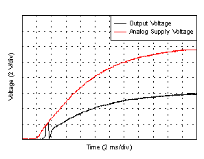 Figure 21. Power-On Response Prior to Programming the Nonvolatile Memory
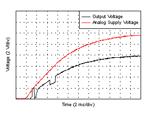 Figure 23. Power-On Response with Nonvolatile Memory Programmed for 8-V Output
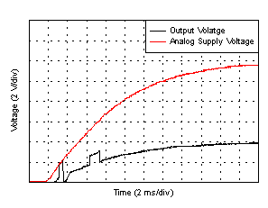 Figure 22. Power-On Response with Nonvolatile Memory Programmed for 4-V Output
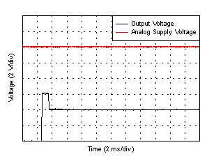 Figure 24. Output Response to a General-Call Reset