ZHCSCF9 May 2014 BUF16821-Q1
PRODUCTION DATA.
- 1 特性
- 2 应用范围
- 3 说明
- 4 修订历史记录
- 5 Pin Configuration and Functions
- 6 Specifications
-
7 Detailed Description
- 7.1 Overview
- 7.2 Functional Block Diagram
- 7.3 Feature Description
- 7.4 Device Functional Modes
- 7.5 Programming
- 7.6 Register Maps
- 8 Application and Implementation
- 9 Power Supply Recommendations
- 10Layout
- 11器件和文档支持
- 12机械封装和可订购信息
7 Detailed Description
7.1 Overview
The BUF16821-Q1 programmable voltage reference allows fast and easy adjustment of 16 programmable gamma reference outputs and two VCOM outputs, each with 10-bit resolution. The device is programmed through a high-speed, I2C interface. The final gamma and VCOM values can be stored in the onboard, nonvolatile memory. To allow for programming errors or liquid crystal display (LCD) panel rework, the device supports up to 16 write operations to the onboard memory. The device has two separate memory banks, allowing simultaneous storage of two different gamma curves to facilitate dynamic switching between gamma curves. Figure 19 illustrates a typical configuration of the device.
7.2 Functional Block Diagram

7.3 Feature Description
7.3.1 Two-Wire Bus Overview
The device communicates over an industry-standard, two-wire interface to receive data in slave mode. This standard uses a two-wire, open-drain interface that supports multiple devices on a single bus. Bus lines are driven to a logic low level only. The device that initiates the communication is called a master, and the devices controlled by the master are slaves. The master generates the serial clock on the clock signal line (SCL), controls the bus access, and generates the start and stop conditions.
To address a specific device, the master initiates a start condition by pulling the data signal line (SDA) from a high to a low logic level while SCL is high. All slaves on the bus shift in the slave address byte on the SCL rising edge, with the last bit indicating whether a read or write operation is intended. During the ninth clock pulse, the slave being addressed responds to the master by generating an acknowledge and pulling SDA low.
Data transfer is then initiated and eight bits of data are sent, followed by an acknowledge bit. During data transfer, SDA must remain stable while SCL is high. Any change in SDA while SCL is high is interpreted as a start or stop condition.
When all data are transferred, the master generates a stop condition, indicated by pulling SDA from low to high while SCL is high. The device can act only as a slave device and therefore never drives SCL. SCL is an input only for the BUF16821-Q1.
7.3.2 Data Rates
The two-wire bus operates in one of three speed modes:
- Standard: allows a clock frequency of up to 100 kHz;
- Fast: allows a clock frequency of up to 400 kHz; and
- High-speed mode (also called Hs mode): allows a clock frequency of up to 2.7 MHz.
The device is fully compatible with all three modes. No special action is required to use the device in standard or fast modes, but high-speed mode must be activated. To activate high-speed mode, send a special address byte of 00001 xxx, with SCL ≤ 400 kHz, following the start condition; where xxx are bits unique to the Hs-capable master, which can be any value. This byte is called the Hs master code. Table 1 provides a reference for the high-speed mode command code. (Note that this configuration is different from normal address bytes—the low bit does not indicate read or write status.) The device responds to the high-speed command regardless of the value of these last three bits. The device does not acknowledge this byte; the communication protocol prohibits acknowledgment of the Hs master code. Upon receiving a master code, the device switches on its Hs mode filters, and communicates at up to 2.7 MHz. Additional high-speed transfers may be initiated without resending the Hs mode byte by generating a repeat start without a stop. The device switches out of Hs mode with the next stop condition.
Table 1. Quick-Reference of Command Codes
| COMMAND | CODE |
|---|---|
| General-call reset | Address byte of 00h followed by a data byte of 06h. |
| High-speed mode | 00001xxx, with SCL ≤ 400 kHz; where xxx are bits unique to the Hs-capable master. This byte is called the Hs master code. |
7.3.3 General-Call Reset and Power-Up
The device responds to a general-call reset, which is an address byte of 00h (0000 0000) followed by a data byte of 06h (0000 0110). The device acknowledges both bytes. Table 1 provides a reference for the general-call reset command code. Upon receiving a general-call reset, the device performs a full internal reset, as though it was powered off and then on. The device always acknowledges the general-call address byte of 00h (0000 0000), but does not acknowledge any general-call data bytes other than 06h (0000 0110).
The device automatically performs a reset when powered up. As part of the reset, the device is configured for all outputs to change to the last programmed nonvolatile memory values, or 1000000000 if the nonvolatile memory values are not programmed.
7.3.4 Output Voltage
The buffer output values are determined by the analog supply voltage (VS) and the decimal value of the binary input code used to program that buffer. The value is calculated using Equation 1:

The device outputs are capable of a full-scale voltage output change in typically 5 μs; no intermediate steps are required.
7.3.5 Updating the DAC Output Voltages
Updating the digital-to-analog converter (DAC) and the VCOM register is not the same as updating the DAC and VCOM output voltage because the device features a double-buffered register structure. There are two methods for updating the DAC and VCOM output voltages.
Method 1: Method 1 is used when the DAC and VCOM output voltage are desired to change immediately after writing to a DAC register. For each write transaction, the master sets data bit 15 to a 1. The DAC and VCOM output voltage update occurs after receiving the 16th data bit for the currently-written register.
Method 2: Method 2 is used when all DAC and VCOM output voltages are desired to change at the same time. First, the master writes to the desired DAC and VCOM channels with data bit 15 a 0. Then, when writing the last desired DAC and VCOM channel, the master sets data bit 15 to a 1. All DAC and VCOM channels are updated at the same time after receiving the 16th data bit.
7.3.6 DIE_ID and DIE_REV Registers
The user can verify the presence of the BUF16821-Q1 in the system by reading from address 111101. When read at this address, the BUF16821-Q1A returns 0101100100100111 and the BUF16821-Q1B returns 0101100100100100.
The user can also determine the die revision of the device by reading from register 111100. The device returns 0000000000000000 when a RevA die is present. RevB is designated by 0000000000000001, and so on.
7.3.7 Read and Write Operations
Read and write operations can be done for a single DAC and VCOM or for multiple DACs and VCOMs. Writing to a DAC and VCOM register differs from writing to the nonvolatile memory. Bits D15–D14 of the most significant byte of data determine if data are written to the DAC and VCOM register or the nonvolatile memory.
7.3.7.1 Read and Write: DAC and VCOM Register (Volatile Memory)
The device is able to read from a single DAC and VCOM, or multiple DACs and VCOMs, or write to the register of a single DAC and VCOM, or multiple DACs and VCOMs in a single communication transaction. The DAC pointer addresses begin with 000000 (which corresponds to OUT1) through 001111 (which corresponds to OUT16). Addresses 010010 and 010011 are VCOM1 and VCOM2, respectively.
Write commands are performed by setting the read and write bit low. Setting the read or write bit high performs a read transaction.
7.3.7.2 Writing: DAC and VCOM Register (Volatile Memory)
To write to a single DAC and VCOM register:
- Send a start condition on the bus.
- Send the device address and read and write bit = low. The device acknowledges this byte.
- Send a DAC and VCOM pointer address byte. Set bit D7 = 0 and D6 = 0. Bits D5–D0 are the DAC and VCOM address. Although the device acknowledges 000000 through 010111, data are stored and returned only from these addresses:
- 000000 through 001111
- 010010 through 010011
- Send two bytes of data for the specified register. Begin by sending the most significant byte first (bits D15–D8, of which only bits D9 and D8 are used, and bits D15–D14 must not be 01), followed by the least significant byte (bits D7–D0). The register is updated after receiving the second byte.
- Send a stop or start condition on the bus.
The device acknowledges each data byte. If the master terminates communication early by sending a stop or start condition on the bus, the specified register is not updated. Updating the DAC and VCOM register is not the same as updating the DAC and VCOM output voltage; see the Updating the DAC Output Voltages section.
The process of updating multiple DAC and VCOM registers begins the same as when updating a single register. However, instead of sending a stop condition after writing the addressed register, the master continues to send data for the next register. The device automatically and sequentially steps through subsequent registers as additional data are sent. The process continues until all desired registers are updated or a stop or start condition is sent.
To write to multiple DAC and VCOM registers:
- Send a start condition on the bus.
- Send the device address and read or write bit = low. The device acknowledges this byte.
- Send either the OUT1 pointer address byte to start at the first DAC, or send the pointer address byte for whichever DAC and VCOM is the first in the sequence of DACs and VCOMs to be updated. The device begins with this DAC and VCOM and steps through subsequent DACs and VCOMs in sequential order.
- Send the bytes of data; begin by sending the most significant byte (bits D15–D8, of which only bits D9 and D8 have meaning, and bits D15–D14 must not be 01), followed by the least significant byte (bits D7–D0). The first two bytes are for the DAC and VCOM addressed in the previous step. The DAC and VCOM register is automatically updated after receiving the second byte. The next two bytes are for the following DAC and VCOM. That DAC and VCOM register is updated after receiving the fourth byte. This process continues until the registers of all following DACs and VCOMs are updated. The device continues to accept data for a total of 18 DACs; however, the two data sets following the 16th data set are meaningless. The 19th and 20th data sets apply to VCOM1 and VCOM2. The write disable bit cannot be accessed using this method. This bit must be written to using the write to a single DAC register procedure.
- Send a stop or start condition on the bus.
The device acknowledges each byte. To terminate communication, send a stop or start condition on the bus. Only DAC registers that have received both bytes of data are updated.
7.3.7.3 Reading: DAC, VCOM, Other Register (Volatile Memory)
Reading a register returns the data stored in that DAC, VCOM, other register.
To read a single DAC, VCOM, other register:
- Send a start condition on the bus.
- Send the device address and read or write bit = low. The device acknowledges this byte.
- Send the DAC, VCOM, other pointer address byte. Set bit D7 = 0 and D6 = 0; bits D5–D0 are the DAC, VCOM, other address. Note that the device stores and returns data only from these addresses:
- 000000 through 001111
- 010010
- 010011
- 111100 through 111111
- Send a start or stop and start condition.
- Send the correct device address and read or write bit = high. The device acknowledges this byte.
- Receive two bytes of data. These bytes are for the specified register. The most significant byte (bits D15–D8) is received first; next is the least significant byte (bits D7–D0). In the case of DAC and VCOM channels, bits D15–D10 have no meaning.
- Acknowledge after receiving the first byte.
- Send a stop or start condition on the bus or do not acknowledge the second byte to end the read transaction.
Communication may be terminated by sending a premature stop or start condition on the bus, or by not acknowledging.
To read multiple registers:
- Send a start condition on the bus.
- Send the device address and read or write bit = low. The device acknowledges this byte.
- Send either the OUT1 pointer address byte to start at the first DAC, or send the pointer address byte for whichever register is the first in the sequence of DACs and VCOMs to be read. The device begins with this DAC and VCOM and steps through subsequent DACs and VCOMs in sequential order.
- Send a start or stop and start condition on the bus.
- Send the correct device address and read or write bit = high. The device acknowledges this byte.
- Receive two bytes of data. These bytes are for the specified DAC and VCOM. The first received byte is the most significant byte (bits D15–D8; only bits D9 and D8 have meaning), next is the least significant byte (bits D7–D0).
- Acknowledge after receiving each byte of data.
- When all desired DACs are read, send a stop or start condition on the bus.
Communication may be terminated by sending a premature stop or start condition on the bus, or by not sending the acknowledge bit. Reading the DieID, DieRev, and MaxBank registers is not supported in this mode of operation (these values must be read using the single register read method).
7.3.7.4 Write: Nonvolatile Memory for the DAC Register
The device is able to write to the nonvolatile memory of a single DAC and VCOM in a single communication transaction. In contrast to the BUF20820, writing to multiple nonvolatile memory words in a single transaction is not supported. Valid DAC and VCOM pointer addresses begin with 000000 (which corresponds to OUT1) through 001111 (which corresponds to OUT16). Addresses 010010 and 010011 are VCOM1 and VCOM2, respectively.
When programming the nonvolatile memory, the analog supply voltage must be between 9 V and 20 V. Write commands are performed by setting the read or write bit low.
To write to a single nonvolatile register:
- Send a start condition on the bus.
- Send the device address and read or write bit = low. The device acknowledges this byte. Although the device acknowledges 000000 through 010111, data are stored and returned only from these addresses:
- 000000 through 001111
- 010010 and 010011
- Send a DAC and VCOM pointer address byte. Set bit D7 = 0 and D6 = 0. Bits D5–D0 are the DAC and VCOM address.
- Send two bytes of data for the nonvolatile register of the specified DAC and VCOM. Begin by sending the most significant byte first (bits D15–D8, of which only bits D9 and D8 are data bits, and bits D15–D14 must be 01), followed by the least significant byte (bits D7–D0). The register is updated after receiving the second byte.
- Send a stop condition on the bus.
The device acknowledges each data byte. If the master terminates communication early by sending a stop or start condition on the bus, the specified nonvolatile register is not updated. Writing a nonvolatile register also updates the DAC and VCOM register and output voltage.
The DAC and VCOM register and DAC and VCOM output voltage are updated immediately, while the programming of the nonvolatile memory takes up to 250 μs. When a nonvolatile register write command is issued, no communication with the device should take place for at least 250 μs. Writing or reading over the serial interface while the nonvolatile memory is being written jeopardizes the integrity of the data being stored.
7.3.7.5 Read: Nonvolatile Memory for the DAC Register
To read the data present in nonvolatile register for a particular DAC and VCOM channel, the master must first issue a general acquire command, or a single acquire command with the appropriate DAC and VCOM channel chosen. This action updates both the DAC and VCOM registers and DAC and VCOM output voltages. The master may then read from the appropriate DAC and VCOM register as described earlier.
 Figure 11. Write DAC Register Timing
 Figure 13. Write Nonvolatile Register Timing
 Figure 15. General-Call Reset Timing
 Figure 12. Read Register Timing
 Figure 14. Acquire Operation Timing
 Figure 16. High-Speed Mode Timing
7.3.8 Output Protection
The device output stages can safely source and sink the current levels indicated in Figure 2 and Figure 3. However, there are other modes where precautions must be taken to prevent the output stages from being damaged by excessive current flow. The outputs (OUT1 through OUT16, VCOM1 and VCOM2) include electrostatic discharge (ESD) protection diodes, as shown in Figure 17. Normally, these diodes do not conduct and are passive during typical device operation. Unusual operating conditions can occur where the diodes may conduct, potentially subjecting them to high, even damaging current levels. These conditions are most likely to occur when a voltage applied to an output exceeds (VS) + 0.5 V, or drops below GND – 0.5 V.
One common scenario where this condition can occur is when the output pin is connected to a sufficiently large capacitor and the device power-supply source (VS) is suddenly removed. Removing the power-supply source allows the capacitor to discharge through the current-steering diodes. The energy released during the high current flow period causes the power dissipation limits of the diode to be exceeded. Protection against the high current flow may be provided by placing current-limiting resistors in series with the output; see Figure 19. Select a resistor value that restricts the current level to the maximum rating for the particular pin.
 Figure 17. Output Pins ESD Protection Current-Steering Diodes
7.4 Device Functional Modes
7.4.1 End-User Selected Gamma Control
The device is well-suited for providing two levels of gamma control by using the BKSEL pin because the device has two banks of nonvolatile memory, as shown in Figure 18. When the state of the BKSEL pin changes, the device updates all 18 programmable buffer outputs simultaneously after 750 μs (±80 μs).
To update all 18 programmable output voltages simultaneously via hardware, toggle the BKSEL pin to switch between gamma curve 0 (stored in Bank0) and gamma curve 1 (stored in Bank1).
All DAC and VCOM registers and output voltages are updated simultaneously after approximately 750 μs.
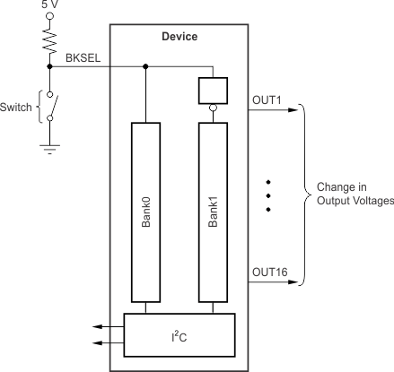 Figure 18. Gamma Control
7.4.2 Dynamic Gamma Control
Dynamic gamma control is a technique used to improve the picture quality in LCD television applications. This technique typically requires switching gamma curves between frames. Using the BKSEL pin to switch between two gamma curves does not often provide good results because of the 750 μs required to transfer the data from the nonvolatile memory to the DAC register. However, dynamic gamma control can still be accomplished by storing two gamma curves in an external electrically erasable programmable read-only memory (EEPROM) and writing directly to the DAC register (volatile).
The double register input structure saves programming time by allowing updated DAC values to be pre-stored into the first register bank. Storage of this data can occur while a picture is still being displayed. Because the data are only stored into the first register bank, the DAC and VCOM output values remain unchanged—the display is unaffected. At the beginning or the end of a picture frame, the DAC and VCOM outputs (and therefore, the gamma voltages) can be quickly updated by writing a 1 in bit 15 of any DAC and VCOM register. For details on the operation of the double register input structure, see the Updating the DAC Output Voltages section.
To update all 18 programmable output voltages simultaneously via software, perform the following actions:
STEP 1: Write to registers 1–18 with bit 15 always 0.
STEP 2: Write any DAC and VCOM register a second time with identical data. Make sure that bit 15 is set to 1. All DAC and VCOM channels are updated simultaneously after receiving the last bit of data.
7.5 Programming
7.5.1 Addressing the Device
The device address 111010x, where x is the state of the A0 pin. When the A0 pin is low, the device acknowledges on address 74h (1110100). If the A0 pin is high, the device acknowledges on address 75h (1110101). Table 2 shows the A0 pin settings and device address options.
Other valid addresses are possible through a simple mask change. Contact your TI representative for information.
Table 2. Quick-Reference of Device Addresses
| DEVICE, COMPONENT (Device Address) |
ADDRESS |
|---|---|
| A0 pin is low (device acknowledges on address 74h) |
1110100 |
| A0 pin is high (device acknowledges on address 75h) |
1110101 |

7.5.2 Nonvolatile Memory
7.5.2.1 BKSEL Pin
The device has 16x rewrite capability of the nonvolatile memory. Additionally, the device is capable of storing two distinct gamma curves in two different nonvolatile memory banks, each of which has 16x rewrite capability. One of the two available banks is selected using the external input pin, BKSEL. When this pin is low, Bank0 is selected; when this pin is high, Bank1 is selected.
When the BKSEL pin changes state, the device acquires the last programmed DAC and VCOM values from the nonvolatile memory associated with this newly chosen bank. At power-up, the state of the BKSEL pin determines which memory bank is selected.
The I2C master can also update (acquire) the DAC registers with the last programmed nonvolatile memory values using software control. The bank to be acquired depends on the state of BKSEL.
7.5.2.2 General Acquire Command
A general acquire command is used to update all registers and DAC and VCOM outputs to the last programmed values stored in nonvolatile memory. A single-channel acquire command updates only the register and DAC and VCOM output of the DAC and VCOM corresponding to the DAC and VCOM address used in the single-channel acquire command.
These are the steps of the sequence to initiate a general channel acquire:
- Be sure BKSEL is in its desired state and is stable for at least 1 ms.
- Send a start condition on the bus.
- Send the appropriate device address (based on A0) and the read or write bit = low. The device acknowledges this byte.
- Send a DAC and VCOM pointer address byte. Set bit D7 = 1 and D6 = 0. Bits D5–D0 are any valid DAC and VCOM address. Although the device acknowledges 000000 through 010111, data are stored and returned only from these addresses:
- 000000 through 001111
- 010010 and 010011
- Send a stop condition on the bus.
Approximately 750 μs (±80 μs) after issuing this command, all DAC and VCOM registers and DAC and VCOM output voltages change to the respective, appropriate nonvolatile memory values.
7.5.2.3 Single-Channel Acquire Command
These are the steps to initiate a single-channel acquire:
- Be sure BKSEL is in its desired state and is stable for at least 1 ms.
- Send a start condition on the bus.
- Send the device address (based on A0) and read or write bit = low. The device acknowledges this byte.
- Send a DAC and VCOM pointer address byte using the DAC and VCOM address corresponding to the output and register to update with the OTP memory value. Set bit D7 = 0 and D6 = 1. Bits D5–D0 are the DAC and VCOM address. Although the device acknowledges 000000 through 010111, data are stored and returned only from these addresses:
- 000000 through 001111
- 010010 and 010011
- Send a stop condition on the bus.
Approximately 36 μs (±4 μs) after issuing this command, the specified DAC and VCOM register and DAC and VCOM output voltage change to the appropriate OTP memory value.
7.5.2.4 MaxBank
The device can provide the user with the number of times the nonvolatile memory of a particular DAC and VCOM channel nonvolatile memory is written to for the current memory bank. This information is provided by reading the register at pointer address 111111.
There are two ways to update the MaxBank register:
- After initiating a single acquire command, the device updates the MaxBank register with a code corresponding to how many times that particular channel memory is written to.
- Following a general acquire command, the device updates the MaxBank register with a code corresponding to the maximum number of times the most used channel (OUT1–16 and VCOMs) is written to.
MaxBank is a read-only register and is only updated by performing a general- or single-channel acquire.
Table 3 shows the relationship between the number of times the nonvolatile memory is programmed and the corresponding state of the MaxBank Register.
Table 3. MaxBank Details
| NUMBER OF TIMES WRITTEN TO | RETURNS CODE |
|---|---|
| 0 | 0000 |
| 1 | 0000 |
| 2 | 0001 |
| 3 | 0010 |
| 4 | 0011 |
| 5 | 0100 |
| 6 | 0101 |
| 7 | 0110 |
| 8 | 0111 |
| 9 | 1000 |
| 10 | 1001 |
| 11 | 1010 |
| 12 | 1011 |
| 13 | 1100 |
| 14 | 1101 |
| 15 | 1110 |
| 16 | 1111 |
7.5.2.5 Parity Error Correction
The device provides single-bit parity error correction for data stored in the nonvolatile memory to provide increased reliability of the nonvolatile memory. If a single bit of nonvolatile memory for a channel fails, the device corrects for the failure and updates the appropriate DAC with the intended value when its memory is acquired.
If more than one bit of nonvolatile memory for a channel fails, the device does not correct for it, and updates the appropriate DAC and VCOM with the default value of 1000000000.
7.6 Register Maps
Table 4. DAC Register Pointer Addresses
| DAC REGISTER | POINTER ADDRESS |
|---|---|
| OUT1 | 000000 |
| OUT2 | 000001 |
| OUT3 | 000010 |
| OUT4 | 000011 |
| OUT5 | 000100 |
| OUT6 | 000101 |
| OUT7 | 000110 |
| OUT8 | 000111 |
| OUT9 | 001000 |
| OUT10 | 001001 |
| OUT11 | 001010 |
| OUT12 | 001011 |
| OUT13 | 001100 |
| OUT14 | 001101 |
| OUT15 | 001110 |
| OUT16 | 001111 |
| VCOM1 | 010010 |
| VCOM2 | 010011 |
| OTHER REGISTER | POINTER ADDRESS |
| Die_Rev | 111100 |
| Die_ID | 111101 |
| MaxBank | 111111 |