ZHCSHU6L march 2018 – august 2023 BQ77915
PRODUCTION DATA
- 1
- 1 特性
- 2 应用
- 3 说明
- 4 Revision History
- 5 说明(续)
- 6 Device Comparison Table
- 7 Pin Configuration and Functions
- 8 Specifications
-
9 Detailed Description
- 9.1 Overview
- 9.2 Functional Block Diagram
- 9.3
Feature Description
- 9.3.1 Protection Summary
- 9.3.2
Fault Operation
- 9.3.2.1 Operation in OV
- 9.3.2.2 Operation in UV
- 9.3.2.3 Operation in OW
- 9.3.2.4 Operation in OCD1
- 9.3.2.5 Operation in OCD2
- 9.3.2.6 Programming the OCD1/2 Delay Using the OCDP Pin
- 9.3.2.7 Operation in SCD
- 9.3.2.8 Operation in OCC
- 9.3.2.9 Overcurrent Recovery Timer
- 9.3.2.10 Load Detection and Load Removal Detection
- 9.3.2.11 Operation in OTC
- 9.3.2.12 Operation in OTD
- 9.3.2.13 Operation in UTC
- 9.3.2.14 Operation in UTD
- 9.3.3 Protection Response and Recovery Summary
- 9.3.4 Cell Balancing
- 9.3.5 HIBERNATE Mode Operation
- 9.3.6 Configuration CRC Check and Comparator Built-In-Self-Test
- 9.3.7 Fault Detection Method
- 9.3.8 State Comparator
- 9.3.9 DSG FET Driver Operation
- 9.3.10 CHG FET Driver Operation
- 9.3.11 External Override of CHG and DSG Drivers
- 9.3.12 Configuring 3-Series, 4-Series, or 5-Series Modes
- 9.3.13 Stacking Implementations
- 9.3.14 Zero-Volt Battery Charging Inhibition
- 9.4 Device Functional Modes
-
10Application and Implementation
- 10.1
Application Information
- 10.1.1 Recommended System Implementation
- 10.2 Typical Application
- 10.1
Application Information
- 11Power Supply Recommendations
- 12Layout
- 13Device and Documentation Support
- 14Mechanical, Packaging, and Orderable Information
9.3.5 HIBERNATE Mode Operation
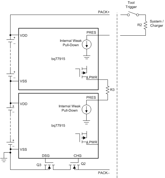
 Figure 9-4 HIBERNATE Mode Simplified Schematic 1
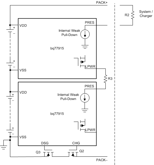
 Figure 9-5 HIBERNATE Mode Simplified Schematic 2
The BQ77915 device has two dedicated pins (PRES and LPWR) for HIBERNATE mode operation. Most of the internal circuitry is turned off in HIBERNATE mode to save power. Charge and discharge FETs are turned off and all fault protections are disabled.
The PRES pin has an internal pulldown connected to the pin, which pulls PRES low. When the PRES pin is left floating (the system or charger is not connected to the pack), the load is not connected, and the device is not in any fault condition, the device enters HIBERNATE mode after tPRES_DEG_ENT time. Once in HIBERNATE mode, the system or the charger should drive this pin high (>VPRESH) through the resistor R2 for NORMAL mode operation. When the battery pack (in HIBERNATE mode) is inserted to the tool/system or when a charger is connected to the pack, the system has to provide a pull-up to the PRES pin, which puts the device back to NORMAL mode. The device will exit HIBERNATE mode after a tPRES_DEG_EXT deglitch time.
In a stacked configuration, connect the LPWR pin of an upper device to the PRES pin of a lower device through the resistor R3.