ZHCSNP0A august   2020  – march 2021 BQ25171-Q1

PRODUCTION DATA  

  1.   1
  2. 特性
  3. 应用
  4. 说明
  5. Revision History
  6. Pin Configuration and Functions
  7. Specifications
    1. 6.1 Absolute Maximum Ratings
    2. 6.2 ESD Ratings
    3. 6.3 Recommended Operating Conditions
    4. 6.4 Thermal Information
    5. 6.5 Electrical Characteristics
    6. 6.6 Timing Requirements
    7. 6.7 典型特性
  8. Detailed Description
    1. 7.1 Overview
    2. 7.2 Functional Block Diagram
    3. 7.3 Feature Description
      1. 7.3.1 Device Power Up from Input Source
        1. 7.3.1.1 ISET Pin Detection
        2. 7.3.1.2 CHM_TMR Pin Detection
        3. 7.3.1.3 VSET Pin Detection
        4. 7.3.1.4 Charger Power Up
      2. 7.3.2 Battery Charging Features
        1. 7.3.2.1 Lithium-Ion Battery Charging Profile
          1. 7.3.2.1.1 NiMH Battery Charging Profile
        2. 7.3.2.2 Charge Termination and Battery Recharge
        3. 7.3.2.3 Charging Safety Timers
        4. 7.3.2.4 Battery Cold, Hot Temperature Qualification (TS Pin)
      3. 7.3.3 Status Outputs (STAT1, STAT2)
        1. 7.3.3.1 Charging Status Indicator (STAT1, STAT2)
      4. 7.3.4 Protection Features
        1. 7.3.4.1 Input Overvoltage Protection (VIN OVP)
        2. 7.3.4.2 Output Overvoltage Protection (BAT OVP)
        3. 7.3.4.3 Output Overcurrent Protection (BAT OCP)
        4. 7.3.4.4 Thermal Regulation and Thermal Shutdown (TREG and TSHUT)
    4. 7.4 Device Functional Modes
      1. 7.4.1 Shutdown or Undervoltage Lockout (UVLO)
      2. 7.4.2 Sleep Mode
      3. 7.4.3 Active Mode
        1. 7.4.3.1 Standby Mode
      4. 7.4.4 Fault Mode
  9. Application and Implementation
    1. 8.1 Application Information
    2. 8.2 Typical Applications
      1. 8.2.1 1s LiFePO4 Charger Design Example
        1. 8.2.1.1 Design Requirements
        2. 8.2.1.2 Detailed Design Procedure
          1. 8.2.1.2.1 Program the Fast Charge Current, ISET:
          2. 8.2.1.2.2 TS Function
        3. 8.2.1.3 Application Curves
      2. 8.2.2 2s Li-Ion Charger with Power Path Design Example
        1. 8.2.2.1 Design Requirements
      3. 8.2.3 4s NiMH Charger Design Example
        1. 8.2.3.1 Design Requirements
  10. Power Supply Recommendations
  11. 10Layout
    1. 10.1 Layout Guidelines
    2. 10.2 Layout Example
  12. 11Device and Documentation Support
    1. 11.1 Device Support
      1. 11.1.1 第三方产品免责声明
    2. 11.2 Receiving Notification of Documentation Updates
    3. 11.3 支持资源
    4. 11.4 Trademarks
    5. 11.5 静电放电警告
    6. 11.6 术语表
  13. 12Mechanical, Packaging, and Orderable Information

请参考 PDF 数据表获取器件具体的封装图。

机械数据 (封装 | 引脚)
  • DRC|10
散热焊盘机械数据 (封装 | 引脚)

Application Curves

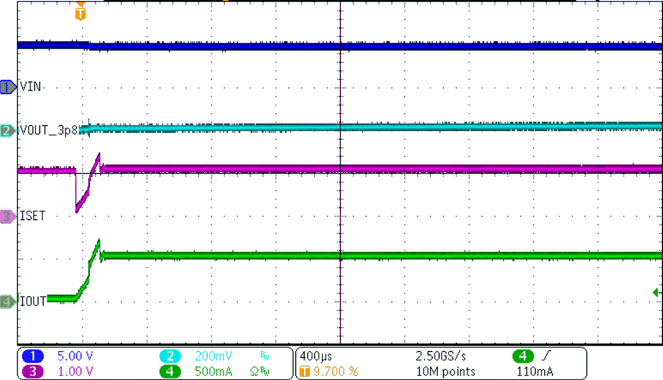
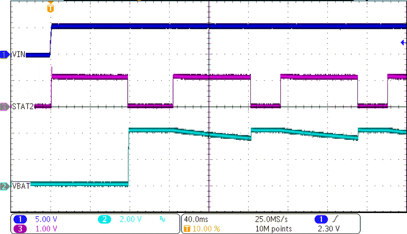
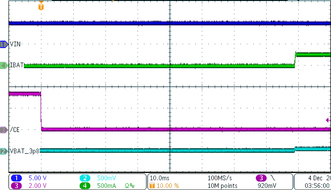
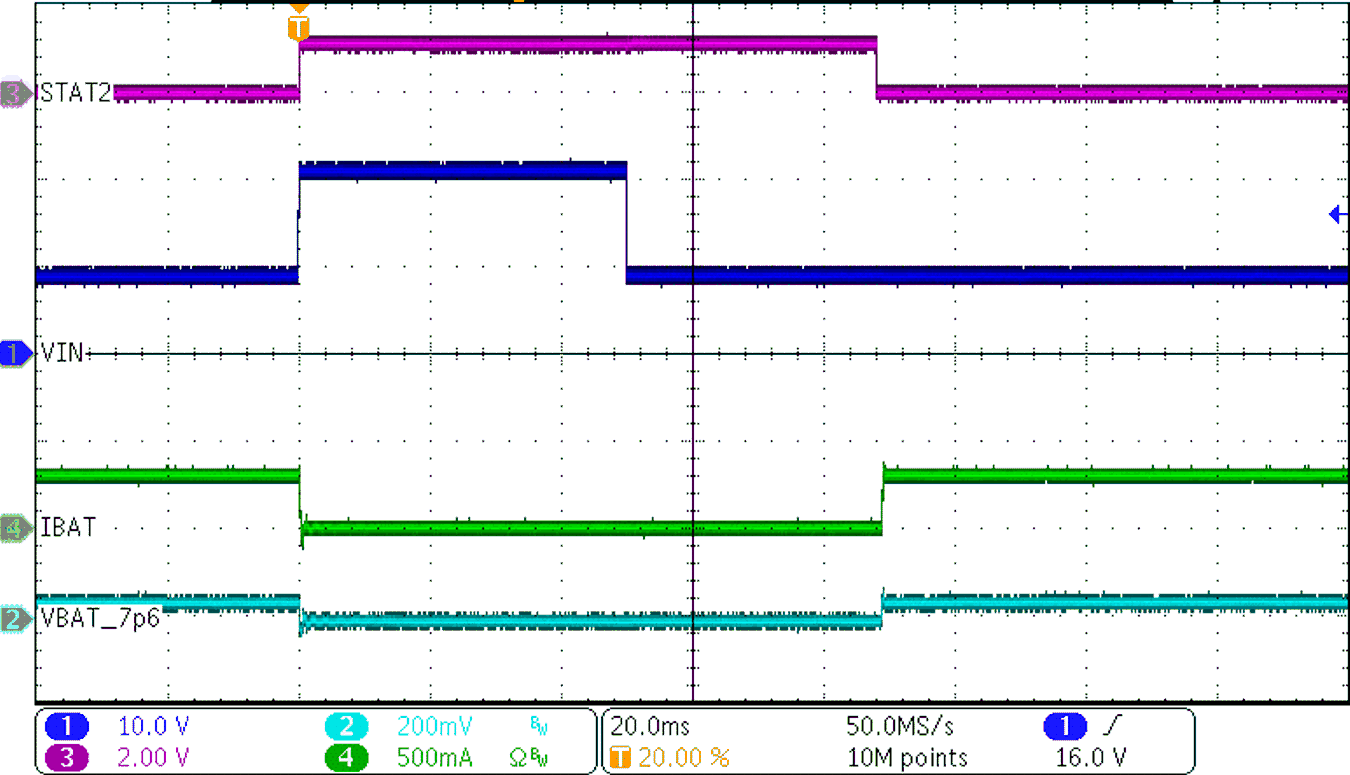
CIN = 1 µF, COUT = 1 µF, VIN = 5 V, VOUT = 3.8 V, ICHG = 250 mA (unless otherwise specified)
GUID-20210211-CA0I-XQ1S-V4T7-Z6B2PWFCWB1C-low.png
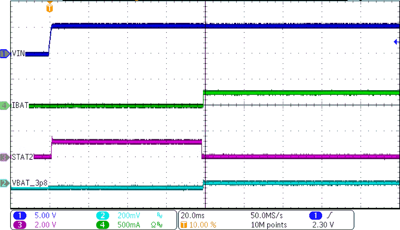
RISET = 1.2 kΩ
Figure 8-2 Power Up with Battery (1-cell Li-Ion)
GUID-20210211-CA0I-SZPG-XD3K-ZXFKK5LW8RFS-low.png
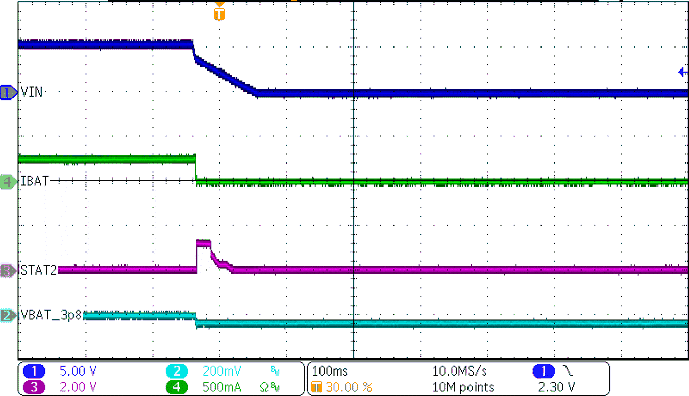
VIN = 5 V → 0 V
Figure 8-4 Power Down
GUID-20210211-CA0I-65KZ-7GDG-H3BRDTJZLT3P-low.png
CE = Low → High
Figure 8-6 Charge Disable
GUID-20210211-CA0I-H7K9-NFLR-7PLDBFRNRS9J-low.png
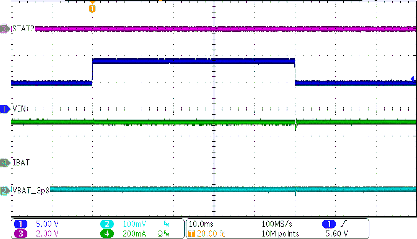
VIN = 5 V → 9 V VOUT = VSET = 4.2 V
Figure 8-8 IN Transient Response
GUID-20210211-CA0I-FXJN-154B-KSXTJXZGVXGZ-low.png
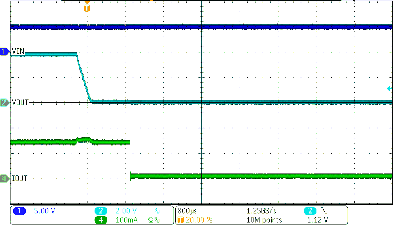
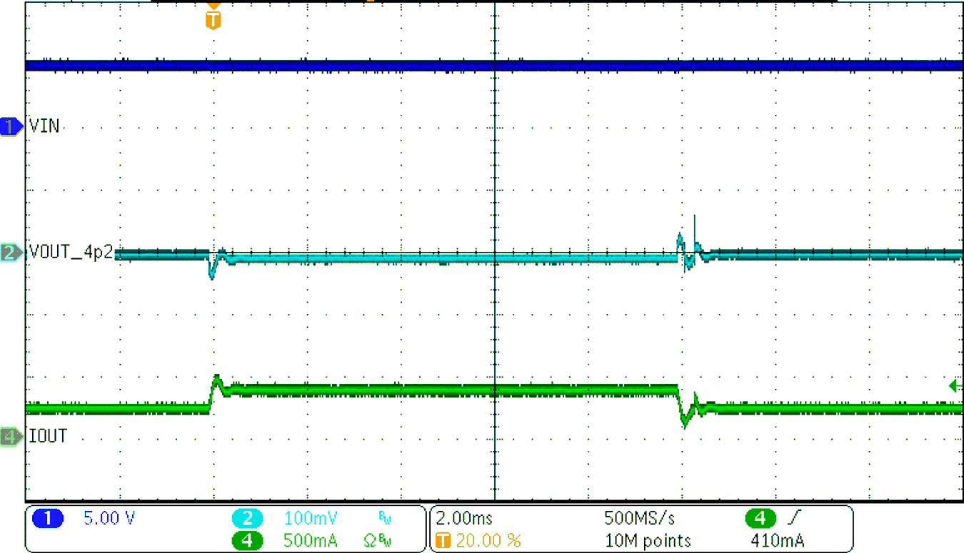
VOUT = VSET = 4.2 V → 0 V
Figure 8-10 OUT Short-Circuit Response
GUID-20210211-CA0I-Q4KZ-P8S6-WDSLSJHGTV4Q-low.png
ISET = 50 mA → 500 mA
Figure 8-12 ISET Change Response
GUID-20210211-CA0I-7FDV-6NMN-DTRDZBZKHWKP-low.png
RISET = 1.2 kΩ OUT = open-circuit
Figure 8-3 Power Up without Battery
GUID-20210211-CA0I-BTTJ-QDKR-VBJ13PKFXTJR-low.png
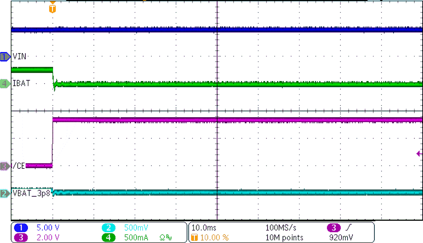
CE = High → Low
Figure 8-5 Charge Enable
GUID-20210211-CA0I-8JHB-XRR9-K3FVXZBJCSS0-low.png
Figure 8-7 IN OVP Response
GUID-20210211-CA0I-2XXR-74NJ-0ZKKBP2SW4ZS-low.png
VOUT = VSET = 4.2 V ISYS = 0 mA → 500 mA
Figure 8-9 OUT Transient Response
GUID-20210211-CA0I-PWX7-462Z-SX9RDWP1MLHM-low.png
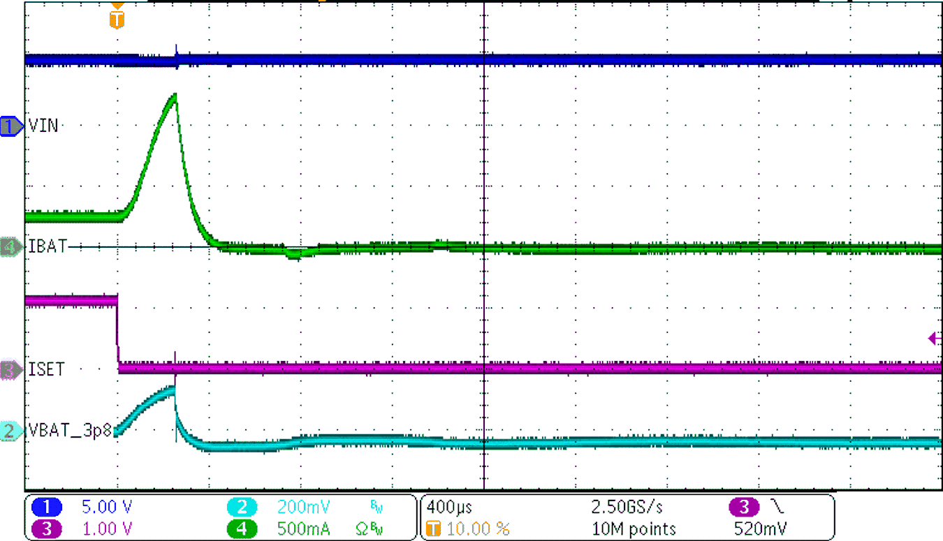
ISET = 1.2 kΩ → 0 Ω
Figure 8-11 ISET Short-Circuit Response
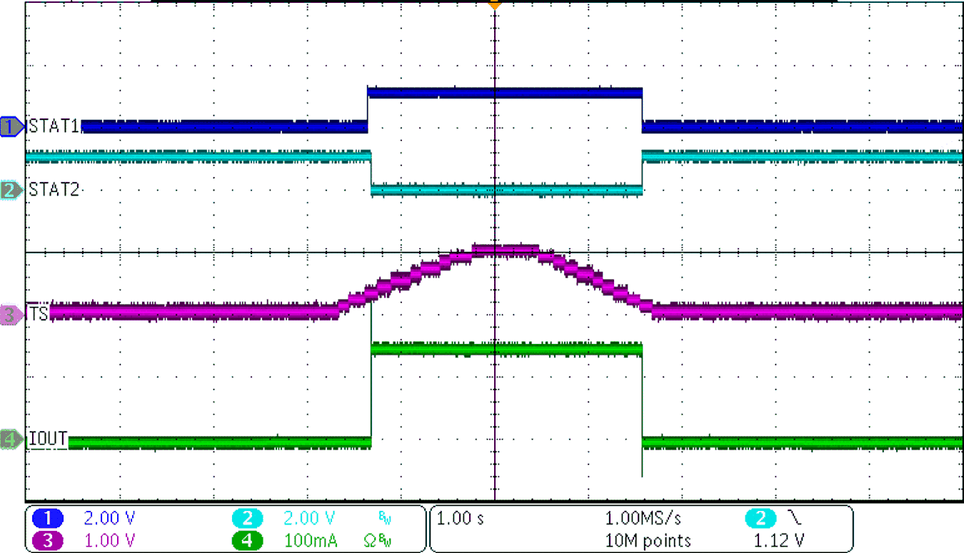
GUID-20210211-CA0I-0RMQ-MDJR-08W8ZXKT4FNK-low.png
Figure 8-13 TS Change Response