SLUS618I August 2004 – December 2014
UNLESS OTHERWISE NOTED, this document contains PRODUCTION DATA.
- 1 Features
- 2 Applications
- 3 Description
- 4 Power Flow Diagram
- 5 Revision History
- 6 Description (continued)
- 7 Device Options
- 8 Pin Configuration and Functions
- 9 Specifications
-
10Detailed Description
- 10.1 Overview
- 10.2 Functional Block Diagram
- 10.3
Feature Description
- 10.3.1 bq24038 Differences
- 10.3.2 Power-Path Management
- 10.3.3 Charge Status Outputs
- 10.3.4 ACPG, USBPG Outputs (Power Good), bq24030/31/32A/35
- 10.3.5 PG Output (Power Good), bq24038
- 10.3.6 CE Input (Chip Enable)
- 10.3.7 VBSEL Input (Battery Voltage Selection), bq24038
- 10.3.8 DPPM Used As A Charge Disable Function
- 10.3.9 Timer Fault Recovery
- 10.3.10 Short-Circuit Recovery
- 10.3.11 LDO Regulator
- 10.4 Device Functional Modes
- 11Application and Implementation
- 12Power Supply Recommendations
- 13Layout
- 14Device and Documentation Support
- 15Mechanical, Packaging, and Orderable Information
封装选项
请参考 PDF 数据表获取器件具体的封装图。
机械数据 (封装 | 引脚)
- RHL|20
散热焊盘机械数据 (封装 | 引脚)
- RHL|20
订购信息
9 Specifications
9.1 Absolute Maximum Ratings(1)
over operating free-air temperature range (unless otherwise noted)| MIN | MAX | UNIT | ||
|---|---|---|---|---|
| Input voltage | AC (DC voltage with respect to VSS) | –0.3 | 18 | V |
| USB (DC voltage with respect to VSS) | –0.3 | 7 | V | |
| Input voltage | BAT, CE, DPPM, ACPG, PSEL, OUT, ISET1, ISET2, STAT1, STAT2, TS, USBPG , PG, VBSEL (all DC voltages with respect to VSS) | –0.3 | 7 | V |
| LDO (DC voltage with respect to VSS) | –0.3 | VO(OUT) + 0.3 | V | |
| TMR | –0.3 | VO(LDO) + 0.3 | V | |
| Input current | AC | 3.5 | A | |
| USB | 1000 | mA | ||
| Output current | OUT | 4 | A | |
| BAT(2) | –4 | 3.5 | A | |
| Output source current (in regulation at 3.3 V LDO) | LDO | 30 | mA | |
| Output sink current | ACPG, STAT1, STAT2, USBPG, PG | 15 | mA | |
| Junction temperature, TJ | –40 | 150 | °C | |
| Lead temperature (soldering, 10 seconds) | 300 | °C | ||
| Storage temperature, Tstg | –65 | 150 | °C | |
(1) Stresses beyond those listed under Absolute Maximum Ratings may cause permanent damage to the device. These are stress ratings only, and functional operation of the device at these or any other conditions beyond those indicated under Recommended Operating Conditions is not implied. Exposure to absolute-maximum-rated conditions for extended periods may affect device reliability. All voltage values are with respect to the network ground terminal unless otherwise noted.
(2) Negative current is defined as current flowing into the BAT pin.
9.2 ESD Ratings
| VALUE | UNIT | |||
|---|---|---|---|---|
| V(ESD) | Electrostatic discharge | Human-body model (HBM), per ANSI/ESDA/JEDEC JS-001(1) | ±1000 | V |
| Charged-device model (CDM), per JEDEC specification JESD22-C101(2) | ±250 | |||
(1) JEDEC document JEP155 states that 500-V HBM allows safe manufacturing with a standard ESD control process. Manufacturing with less than 500-V HBM is possible with the necessary precautions.
(2) JEDEC document JEP157 states that 250-V CDM allows safe manufacturing with a standard ESD control process. Manufacturing with less than 250-V CDM is possible with the necessary precautions.
9.3 Recommended Operating Conditions
| MIN | MAX | UNIT | |||
|---|---|---|---|---|---|
| VCC | Supply voltage (from AC input) (1)(2) | bq24030/31/32A/35, bq24038 (at VBSEL = LOW) | 4.35 | 16 | V |
| bq24038 (at VBSEL = HIGH) | 4.55 | 16 | |||
| VCC | Supply voltage (from USB input) (1) | 4.35 | 6 | ||
| IAC | Input current, AC | 2 | A | ||
| IUSB | Input current, USB | 0.5 | |||
| TJ | Operating junction temperature range | –40 | 125 | °C | |
(1) VCC is defined as the greater of AC or USB input.
(2) Verify that power dissipation and junction temperatures are within limits at maximum VCC .
9.4 Thermal Information
| THERMAL METRIC(1) | bq2403x | UNIT | |
|---|---|---|---|
| RHL | |||
| 20 PINS | |||
| RθJA | Junction-to-ambient thermal resistance | 40.1 | °C/W |
| RθJC(top) | Junction-to-case (top) thermal resistance | 42.0 | |
| RθJB | Junction-to-board thermal resistance | 16.6 | |
| ψJT | Junction-to-top characterization parameter | 0.7 | |
| ψJB | Junction-to-board characterization parameter | 16.6 | |
| RθJC(bot) | Junction-to-case (bottom) thermal resistance | 4.2 | |
(1) For more information about traditional and new thermal metrics, see the IC Package Thermal Metrics application report, SPRA953.
9.5 Dissipation Ratings
| PACKAGE | TA ≤ 40°C POWER RATING |
DERATING FACTOR TA > 40°C |
θJA |
|---|---|---|---|
| 20-pin RHL(1) | 1.81 W | 21 mW/°C | 46.87 °C/W |
(1) This data is based on using the JEDEC High-K board and the exposed die pad is connected to a Cu pad on the board. This is connected to the ground plane by a 2×3 via matrix.
9.6 Electrical Characteristics
over junction temperature range (0°C ≤ TJ ≤ 125°C) and the recommended supply voltage range (unless otherwise noted)| PARAMETER | TEST CONDITIONS | MIN | TYP | MAX | UNIT | ||
|---|---|---|---|---|---|---|---|
| INPUT BIAS CURRENTS | |||||||
| ICC(SPLY) | Active supply current, VCC | VVCC > VVCC(min) | 1 | 2 | mA | ||
| ICC(SLP) | Sleep current (current into BAT pin) | V(AC) < V(BAT), V(USB) < V(BAT), 2.6 V ≤ VI(BAT) ≤ VO(BAT-REG), Excludes load on OUT pin |
2 | 5 | μA | ||
| ICC(AS-STDBY) | AC standby current | VI(AC) ≤ 6 V, Total current into AC pin with chip disabled, Excludes all loads, CE=LOW, after t(CE-HOLDOFF) delay | 200 | ||||
| ICC(USB-STDBY) | USB standby current | Total current into USB pin with chip disabled, Excludes all loads, CE=LOW, after t(CE-HOLDOFF) delay | 200 | ||||
| ICC(BAT-STDBY) | BAT standby current | Total current into BAT pin with AC and/or USB present and chip disabled; Excludes all loads (OUT and LDO), CE=LOW, after t(CE-HOLDOFF) delay, 0°C ≤ TJ ≤ 85°C(1) |
45 | 60 | |||
| IIB(BAT) | Charge done current, BAT | Charge DONE, AC or USB supplying the load | 1 | 5 | |||
| HIGH AC CUTOFF MODE | |||||||
| VCUT-OFF | Input ac cutoff voltage, bq24035 | VI(AC) > 6.8 V, AC FET (Q1) turns off, USB FET (Q3) turns on if USB power present, otherwise BAT FET (Q2) turns on. | 6.1 | 6.4 | 6.8 | V | |
| LDO OUTPUT | |||||||
| VO(LDO) | Output regulation voltage | Active only if AC or USB is present, VI(OUT) ≥ VO(LDO) + (IO(LDO) × RDS(on)) |
3.3 | V | |||
| Regulation accuracy(2) | –5% | 5% | |||||
| IO(LDO) | Output current | 20 | mA | ||||
| RDS(on) | On resistance | OUT to LDO | 50 | Ω | |||
| C(OUT)(3) | Output capacitance | 1 | μF | ||||
| OUT PIN-VOLTAGE REGULATION(4) | |||||||
| VO(OUT-REG) | Output regulation voltage | bq24030/31 | VI(AC) ≥ 6 V+VDO | 6.0 | 6.3 | V | |
| bq24032A | VI(AC) ≥ 4.4 V+VDO | 4.4 | 4.5 | ||||
| bq24038 | VBSEL = HIGH or VBSEL = LOW, VI(AC) > 4.4 V+VDO | 4.4 | 4.5 | ||||
| OUT PIN – DPPM REGULATION | |||||||
| V(DPPM-SET) | DPPM set point(5) | VDPPM-SET < VOUT | 2.6 | 5 | V | ||
| I(DPPM-SET) | DPPM current source | AC or USB present | 95 | 100 | 105 | μA | |
| SF | DPPM scale factor | V(DPPM-REG)= V(DPPM-SET) × SF | 1.139 | 1.150 | 1.162 | ||
| OUT PIN – FET (Q1, Q3, AND Q2) DROP-OUT VOLTAGE (RDSon) | |||||||
| V(ACDO) | AC to OUT dropout voltage(6) | VI(AC) ≥ VCC(min), PSEL = High, II(AC) = 1 A, (IO(OUT)+ IO(BAT)), or no AC |
300 | 475 | mV | ||
| V(USBDO)(13) | USB to OUT dropout voltage | VI(USB) ≥ VCC(min), PSEL = Low, ISET2 = High, II(USB) = 0.4 A, (IO(OUT)+IO(BAT)), or no AC |
140 | 180 | |||
| VI(USB) ≥ VCC(min), PSEL = Low, ISET2 = Low, II(USB) = 0.08 A, (IO(OUT)+ IO(BAT)) |
28 | 36 | |||||
| V(BATDO) | BAT to OUT dropout voltage (discharging) | VI (BAT) ≥ 3 V, Ii(BAT)= 1.0 A, VCC < Vi(BAT) | 40 | 100 | mV | ||
| OUT PIN - BATTERY SUPPLEMENT MODE | |||||||
| VBSUP1 | Enter battery supplement mode (battery supplements OUT current in the presence of input source | VI(BAT)> 2 V | VI(OUT)
≤ VI(BAT) – 60 mV |
V | |||
| VBSUP2 | Exit battery supplement mode | VI(BAT)> 2 V | VI(OUT)
≥ VI(BAT) – 20 mV |
||||
| OUT PIN - SHORT CIRCUIT | |||||||
| IOSH1 | BAT to OUT short-circuit recovery | Current source between BAT to OUT for short-circuit recovery to VI(OUT) ≤ VI(BAT) –200 mV | 10 | mA | |||
| RSHAC | AC to OUT short-circuit limit | VI(OUT) ≤ 1 V | 500 | Ω | |||
| RSHVSB | USB to OUT short-circuit limit | VI(OUT) ≤ 1 V | 500 | ||||
| BAT PIN CHARGING – PRECHARGE | |||||||
| V(LOWV) | Precharge to fast-charge transition threshold | Voltage on BAT | 2.9 | 3 | 3.1 | V | |
| TDGL(F) | Deglitch time for fast-charge to precharge transition(12) | tFALL = 100 ns, 10 mV overdrive, VI(BAT) decreasing below threshold |
22.5 | ms | |||
| IO(PRECHG) | Precharge range | 1 V < VI(BAT) < V(LOWV), t < t(PRECHG), IO(PRECHG) = (K(SET)× V(PRECHG))/ RSET |
10 | 150 | mA | ||
| V(PRECHG) | Precharge set voltage | 1 V < VI(BAT) < V(LOWV), t < t(PRECHG) | 230 | 250 | 270 | mV | |
| BAT PIN CHARGING - CURRENT REGULATION | |||||||
| IO(BAT) | AC battery charge current range(7) | Vi (BAT) > V(LOWV), VI(OUT) - VI (BAT) > V(DO-MAX), PSEL = High IOUT(BAT) = (K(SET) × V(SET) / RSET), VI(OUT) > VO(OUT-REG) + V(DO-MAX) |
100 | 1000 | 1500 | mA | |
| RPBAT | BAT to OUT pullup | Vi (BAT)< 1 V | 1000 | Ω | |||
| RPOUT | AC to OUT and USB to OUT short-circuit pullup | VI(OUT) < 1 V | 500 | ||||
| V(SET) | Battery charge current set voltage(8) | Voltage on ISET1, VVCC ≥ 4.35 V, VI(OUT)- VI(BAT) > V(DO-MAX), VI(BAT) > V(LOWV) |
2.475 | 2.500 | 2.525 | V | |
| K(SET) | Charge current set factor, BAT | 100 mA ≤ IO(BAT) ≤ 1 A | 400 | 425 | 450 | ||
| 10 mA ≤ IO(BAT) ≤ 100 mA(9) | 300 | 450 | 600 | ||||
| USB PIN INPUT CURRENT REGULATION | |||||||
| I(USB) | USB input current range, bq24030/32A/35/38(11) | VI(BAT) > V(LOWV), VI(USB) - VI(BAT) > V(DO-MAX), ISET2= Low, PSEL = Low, or no AC (10) |
100 | mA | |||
| VI(BAT) > V(LOWV), VI(USB) - VI(BAT) > V(DO-MAX), ISET2= High, PSEL = Low, or no AC (11) |
400 | 500 | |||||
| BAT PIN CHARGING VOLTAGE REGULATION, VO (BAT-REG) + V (DO-MAX) < VCC, ITERM < IBAT(OUT) ≤ 1 A | |||||||
| VO(BAT-REG) | Battery charge voltage | bq24030/32A/35 | 4.2 | V | |||
| bq24031 | 4.1 | ||||||
| bq24038 | VBSEL = HI | 4.36 | |||||
| VBSEL = LO | 4.2 | ||||||
| Battery charge voltage regulation accuracy | TA = 25°C | –0.5% | 0.5% | ||||
| –1% | 1% | ||||||
| CHARGE TERMINATION DETECTION | |||||||
| I(TERM) | Charge termination detection range | VI(BAT) < V(RCH), I(TERM) = (K(SET) × V(TERM))/ RSET | 10 | 150 | mA | ||
| V(TERM-AC) | AC-charge termination detection voltage, measured on ISET1 | VI(BAT) > V(RCH) , PSEL = High, ACPG = Low | 235 | 250 | 265 | mV | |
| V(TAPER-USB) | USB-charge termination detection voltage, measured on ISET1 | VI(BAT) > V(RCH), PSEL = Low or PSEL = High and ACPG = High |
95 | 100 | 130 | mV | |
| TDGL(TERM) | Deglitch time for termination detection | tFALL = 100 ns, 10 mV overdrive, ICHG increasing above or decreasing below threshold |
22.5 | ms | |||
| TEMPERATURE SENSE COMPARATORS | |||||||
| VLTF | High voltage threshold | Temp fault at V(TS) > VLTF | 2.465 | 2.500 | 2.535 | V | |
| VHTF | Low voltage threshold | Temp fault at V(TS) < VHTF | 0.485 | 0.500 | 0.515 | V | |
| ITS | Temperature sense current source | 94 | 100 | 106 | μA | ||
| TDGL(TF) | Deglitch time for temperature fault detection(12) | R(TMR) = 50 kΩ, VI(BAT) increasing or decreasing above and below; 100-ns fall time, 10-mv overdrive | 22.5 | ms | |||
| BATTERY RECHARGE THRESHOLD | |||||||
| VRCH | Recharge threshold voltage | VO(BAT-REG)
–0.075 |
VO(BAT-REG)
–0.100 |
VO(BAT-REG)
–0.125 |
V | ||
| TDGL(RCH) | Deglitch time for recharge detection(12) | R(TMR) = 50 kΩ, VI(BAT) increasing or decreasing below threshold, 100-ns fall time, 10-mv overdrive |
22.5 | ms | |||
| STAT1, STAT2. ACPG AND USBPG, PG OPEN DRAIN (OD) OUTPUTS(15) | |||||||
| VOL | Low-level output saturation voltage | IOL = 5 mA, An external pullup resistor ≥ 1 K required. |
0.25 | V | |||
| ILKG | Input leakage current | 1 | 5 | μA | |||
| ISET2, CE, VBSEL INPUTS | |||||||
| VIL | Low-level input voltage | 0 | 0.4 | V | |||
| VIH | High-level input voltage | 1.4 | |||||
| IIL | Low-level input current, CE | –1 | μA | ||||
| IIH | High-level input current, CE | 1 | |||||
| IIL | Low-level input current, ISET2 | VISET2 = 0 V | –20 | ||||
| IIH | High-level input current, ISET2 | VISET2 = VCC | 40 | ||||
| IIL1 | Low-level input current | VBSEL = Low | 6 | 1 | |||
| IIH1 | High-level input current | VBSEL = High | 15 | ||||
| t(CE-HLDOFF) | Holdoff time, CE | CE going low only | 3.3 | 6.2 | ms | ||
| PSEL INPUT | |||||||
| VIL | Low-level input voltage | Falling Hi→Low; 280 K ± 10% applied when low. | 0.975 | 1 | 1.025 | V | |
| VIH | High-level input voltage | Input RPSEL sets external hysteresis | VIL + 0.01 | VIL + 0.024 | V | ||
| IIL | Low-level input current, PSEL | –1 | μA | ||||
| IIH | High-level input current, PSEL | μA | |||||
| TIMERS | |||||||
| K(TMR) | Timer set factor | t(CHG) = K(TMR) × R(TMR) | 0.313 | 0.360 | 0.414 | s/Ω | |
| R(TMR)(14) | External resistor limits | 30 | 100 | kΩ | |||
| t(PRECHG) | Precharge timer | 0.09 × t(CHG) | 0.10 × t(CHG) | 0.11 × t(CHG) | s | ||
| I(FAULT) | Timer fault recovery pullup from OUT to BAT | 1 | kΩ | ||||
| CHARGER SLEEP THRESHOLDS (ACPG , PG, and USBPG THRESHOLDS, LOW → POWER GOOD) | |||||||
| V(SLPENT)(19) | Sleep-mode entry threshold | V(UVLO) ≤ VI(BAT) ≤ VO(BAT-REG), No t(BOOT-UP) delay |
VVCC ≤ VI(BAT) +125 mV |
V | |||
| V(SLPEXIT)(19) | Sleep-mode exit threshold | V(UVLO) ≤ VI(BAT) ≤ VO(BAT-REG), No t(BOOT-UP) delay |
VVCC ≥ VI(BAT) +190 mV |
||||
| t(DEGL) | Deglitch time for sleep mode(16) | R(TMR) = 50 kΩ, V(AC) or V(USB) or decreasing below threshold, 100-ns fall time, 10-mv overdrive |
22.5 | ms | |||
| START-UP CONTROL and USB BOOT-UP | |||||||
| t(BOOT-UP) | Boot-up time | On the first application of USB input power or AC input with PSEL Low | 120 | 150 | 180 | ms | |
| SWITCHING POWER SOURCE TIMING | |||||||
| tSW-BAT | Switching power source from inputs (AC or USB) to battery | Only AC power or USB power applied. Measure from: [xxPG: Lo → Hi to I(xx) > 5 mA], xx = AC or USB I(OUT) = 100 mA, RTRM = 50 K |
50 | μs | |||
| tSW-AC/USB | Switching from AC to USB, or, USB to AC by input source removal. (17) | Measure from: I(AC) < 5 mA to I(USB) > 5 mA or I(USB) < 5 mA → I(AC) > 5 mA; I(OUT) = 100 mA, RTMR = 50 K, ISET2 = hi, ROUT > 15 Ω, VDPPM = 2.5 V |
100 | ||||
| tSW-PSEL | Switching from AC to USB, or USB to AC by toggling PSEL | 50 | 100 | ||||
| THERMAL SHUTDOWN REGULATION(18) | |||||||
| T(SHTDWN) | Temperature trip | TJ (Q1 and Q3 only) | 155 | °C | |||
| Thermal hysteresis | TJ (Q1 and Q3 only) | 30 | |||||
| TJ(REG) | Temperature regulation limit | TJ (Q2) | 115 | 135 | |||
| UVLO | |||||||
| V(UVLO) | Undervoltage lockout | Decreasing VCC | 2.45 | 2.50 | 2.65 | V | |
| Hysteresis | 27 | mV | |||||
(1) This includes the quiescent current for the integrated LDO.
(2) In standby mode (CE low) the accuracy is ±10%.
(3) LDO output capacitor not required but one with a value of 0.1 μF is recommended.
(4) When power is applied to the USB pin and PSEL is low, the USB input is switched straight through to the OUT pin (not regulated). This voltage may drop to the DPPM-OUT threshold or battery voltage (which ever is higher) if the USB input current limit is active.
(5) V(DPPM-SET) is scaled up by the scale factor for controlling the output voltage V(DPPM-REG).
(6) VDO(max), dropout voltage is a function of the FET, RDS(on), and drain current. The dropout voltage increases proportionally to the increase in current.
(7) When input current remains below 2 A, the battery charging current may be raised until the thermal regulation limits the charge current.
(8) For half-charge rate, V(SET) is 1.25 V ± 25 mV for bq24032A/38 only.
(9) Specification is for monitoring charge current via the ISET1 pin during voltage regulation mode, not for a reduced fast-charge level.
(10) With the PSEL= low, the bqTINY III-series defaults to USB charging. If USB input is ≤ VBAT, then the bqTINY III-series charges from the AC input at the USB charge rate. In this configuration, the specification is 80 mA (min) and 100 mA (max).
(11) With the PSEL= low, the bqTINY III-series defaults to USB charging. If USB input is ≤ VBAT, then the bqTINY III-series charges from the AC input at the USB charge rate. In this configuration, the specification is 400 mA (min) and 500 mA (max).
(12) All deglitch periods are a function of the timer setting and is modified in DPPM or thermal regulation modes by the percentages that the program current is reduced.
(13) RDS(on) of USB FET Q3 is calculated by: (VUSB – VOUT) / (IOUT + IBAT) when II(USB) ≤ II(USB-MIN) (FET fully on, not in regulation).
(14) To disable the fast-charge safety timer and charge termination, tie TMR to the LDO pin. Tying the TMR pin high changes the timing resistor from the external value to an internal 50 kΩ ±25%, which can add an additional tolerance to any timed spectification. The TMR pin normally regulates to 2.5 V when the charge current is not restricted by the DPPM or thermal feedback loops. If these loops become active, the TMR pin voltage will be reduced proportionally to the reduction in charge current and the clock frequency will be reduced by the same percentage (timed durations will count down slower, extending their time). The TMR pin is clamped at 0.80 V, for a maximum time extension of 2.5 V ÷ 0.8 V × 100 = 310%.
(15) See Charger Sleep mode for ACPG (VCC = VAC) and USBPG (VCC = VUSB) specifications.
(16) Does not declare sleep mode until after the deglitch time and implement the needed power transfer immediately according to the switching specification.
(17) The power handoff is implemented once the PG pin goes high (removed sources PG) which is when the removed source drops to the battery voltage. If the battery voltage is critically low, the system may lose power unless the system takes control of the PSEL pin and switches to the available power source prior to shutdown. The USB source often has less current available; so, the system may have to reduce its load when switching from AC to USB.
(18) Reaching thermal regulation reduces the charging current. Battery supplement current is not restricted by either thermal regulation or shutdown. Input power FETs turn off during thermal shutdown. The battery FET is only protected by a short-circuit limit which typically does not cause a thermal shutdown (input FETs turning off) by itself.
(19) The IC is considered in sleep mode when both AC and USB are absent (ACPG = USBPG = OPEN DRAIN).
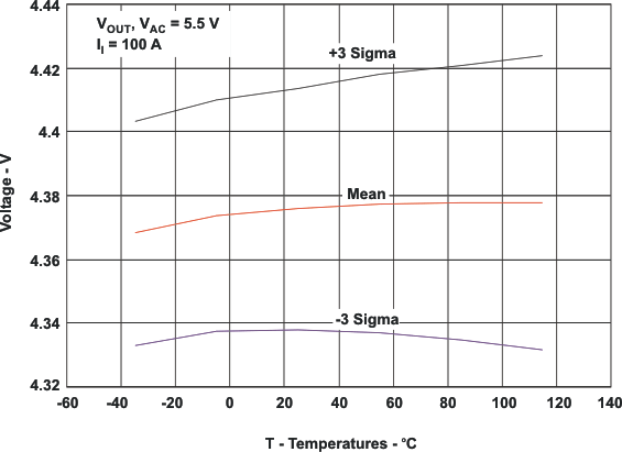
9.7 Typical Characteristics