SLUS618I August 2004 – December 2014
UNLESS OTHERWISE NOTED, this document contains PRODUCTION DATA.
- 1 Features
- 2 Applications
- 3 Description
- 4 Power Flow Diagram
- 5 Revision History
- 6 Description (continued)
- 7 Device Options
- 8 Pin Configuration and Functions
- 9 Specifications
-
10Detailed Description
- 10.1 Overview
- 10.2 Functional Block Diagram
- 10.3
Feature Description
- 10.3.1 bq24038 Differences
- 10.3.2 Power-Path Management
- 10.3.3 Charge Status Outputs
- 10.3.4 ACPG, USBPG Outputs (Power Good), bq24030/31/32A/35
- 10.3.5 PG Output (Power Good), bq24038
- 10.3.6 CE Input (Chip Enable)
- 10.3.7 VBSEL Input (Battery Voltage Selection), bq24038
- 10.3.8 DPPM Used As A Charge Disable Function
- 10.3.9 Timer Fault Recovery
- 10.3.10 Short-Circuit Recovery
- 10.3.11 LDO Regulator
- 10.4 Device Functional Modes
- 11Application and Implementation
- 12Power Supply Recommendations
- 13Layout
- 14Device and Documentation Support
- 15Mechanical, Packaging, and Orderable Information
封装选项
请参考 PDF 数据表获取器件具体的封装图。
机械数据 (封装 | 引脚)
- RHL|20
散热焊盘机械数据 (封装 | 引脚)
- RHL|20
订购信息
11 Application and Implementation
NOTE
Information in the following applications sections is not part of the TI component specification, and TI does not warrant its accuracy or completeness. TI’s customers are responsible for determining suitability of components for their purposes. Customers should validate and test their design implementation to confirm system functionality.
11.1 Application Information
Compared to chargers without dynamic power path management (DPPM), this single-cell LiIon battery charger provides instant system power even with a deeply discharged battery. The maximum charge current is set by ISET2 but the input current limit circuitry, controlled by ISET1 and PSEL pins or the DPPM circuitry can reduce the charge current from the maximum desired value.
11.2 Typical Application
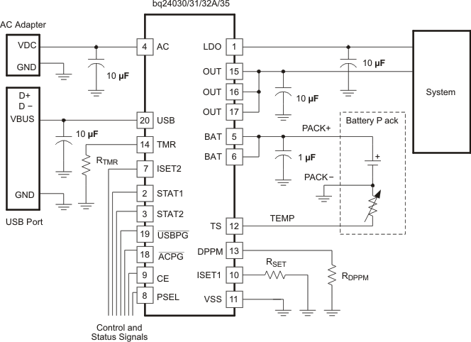 Figure 7. Typical Application Schematic
11.2.1 Design Requirements
A bq24070 (VOUT = 4.4 Vreg) is powered through an AC adaptor with IN input is set for ~5.1 V (1.5 A current limit), I(CHG) = 1 A, V(DPPM-SET) = 3.7 V, V(DPPM-REG) = 1.15 × V(DPPM-SET) = 4.26 V, Mode = H, and USB input is not connected. A 103AT thermistor is inside the battery pack. A 6-hour saftey timeout is desired.
11.2.2 Detailed Design Procedure
The minimum required 0.1 μF capacitors are placed on IN and OUT. Additional 10 μF capacitors are included on IN and OUT to improve load transient response. The recommended (but not required) 33 μF capacitor on BAT is added to allow for operation when no battery is attached. A 0.22 μF capacitor is connected between BAT and ISET1 to improve operation at low charge currents.
Rearranging Equation 5 gives RSET = V(SET) x K(SET) / IO(BAT) = 2.5 V x 425 / 1 A = 1062.5 Ω → 1070 Ω. Per Equation 4, the precharge current is 100 mA and per Equation 10, the termination current is 100 mA. Since MODE is high, in order to prevent the charge current from being reduced by 1/2, ISET2 is tied high.
Rearranging Equation 7 gives RTMR = t(CHG) / K(TMR) gives 6 hrs x 60 min/hr x 60 s/min / 0.360 s/Ω = 60 kΩ → 60.4 kΩ
Rearranging Equation 1 gives RDPPM = V(DPPM-REG) / (I(DPPM) x SF) = 4.26 V / ( 100 μA x 1.15) = 37.044 kΩ →37.4 kΩ. CDPPM of 10 nF was added to prevent the IC from falsely entering short circuit protection at start up.
Not shown are 1.5-kΩ resistors and LEDs pulled up to V(IN) from STAT1, STAT2 and PG.
11.2.2.1 Selecting the Input and Output Capacitors
In most applications, all that is needed is a high-frequency decoupling capacitor on each input (AC and USB). A 0.1-μF ceramic capacitor, placed in close proximity to AC and USB to VSS pins, works well. In some applications depending on the power supply characteristics and cable length, it may be necessary to add an additional 10-μF ceramic capacitor to each input.
The bqTINY III-series only requires a small output capacitor for loop stability. A 0.1-μF ceramic capacitor placed between the OUT and VSS pin is typically sufficient.
The integrated LDO requires a maximum of 1-μF ceramic capacitor on its output. The output does not require a capacitor for a steady-state load but a 0.1-μF minimum capacitance is recommended.
It is recommended to install a minimum of 33-μF capacitor between the BAT pin and VSS (in parallel with the battery). This ensures proper hot plug power up with a no-load condition (no system load or battery attached).
This short-circuit disable feature was implemented mainly for power up when inserting a battery. Because the BAT input voltage rises much faster than the OUT voltage (Vout<Vbat-200 mV), with most any capacitive load on the output, the part can get stuck in short-circuit mode. Placing a 1 nF to 100 nF capacitor between the DPPM pin and ground slows the VDPPM rise time, during power up, and delays the short-circuit protection.
11.2.3 Application Curves
Figure 8 illustrates DPPM and battery supplement modes as the output current (IOUT) is increased; channel 1 (CH1) VAC = 5.4 V; channel 2 (CH2) VOUT; channel 3 (CH3) IOUT = 0 to 2.2 A to 0 A; channel 4 (CH4) VBAT = 3.5 V; I(PGM-CHG) = 1 A. In typical operation, bq24032A (VOUT = 4.4 Vreg), through an AC adaptor overload condition and recovery. The AC input is set for ~5.1 V (1.5 A current limit), I(CHG) = 1 A, V(DPPM-SET) = 3.7 V, V(DPPM-OUT) = 1.15 × V(DPPM-SET) = 4.26 V, VBAT = 3.5 V, PSEL = H, and USB input is not connected. The output load is increased from 0 A to ~2.2 A and back to 0 A as shown in the bottom waveform. As the IOUT load reaches 0.5 A, along with the 1-A charge current, the adaptor starts to current limit, the output voltage drops to the DPPM-OUT threshold of 4.26 V. This is DPPM mode. The AC input tracks the output voltage by the dropout voltage of the AC FET. The battery charge current is then adjusted back as necessary to keep the output voltage from falling any further. Once the output load current exceeds the input current, the battery has to supplement the excess current and the output voltage falls just below the battery voltage by the dropout voltage of the battery FET. This is the battery supplement mode. When the output load current is reduced, the operation described is reversed as shown. If V(DPPM-REG) was set below the battery voltage, during input current limiting, the output falls directly to the battery's voltage.
Under USB operation, when the loads exceeds the programmed input current thresholds a similar pattern is observed. If the output load exceeds the available USB current, the output instantly goes into the battery supplement mode.
Figure 9 illustrates when PSEL is toggled low for 500 μs. Power transfers from AC to USB to AC; channel 1 (CH1) VAC = 5.4 V; channel 2 (CH2) V(USB) = 5 V; channel 3 (CH3) VOUT; output current, IOUT = 0.25 A; channel 4 (CH4) VBAT = 3.5 V; and I(PGM-CHG) = 1 A. When the PSEL went low (1st div), the AC FET opened, and the output fell until the USB FET turned on. Turning off the active source before turning on the replacement source is referred to as break-before-make switching. The rate of discharge on the output is a function of system capacitance and load. Note the cable IR drop in the AC and USB inputs when they are under load. At the 4th division, the output has reached steady-state operation at V(DPPM-REG) (charge current has been reduced due to the limited USB input current). At the 6th division, the PSEL goes high and the USB FET turns off followed by the AC FET turning on. The output returns to its regulated value, and the battery returns to its programmed current level.
Figure 10 illustrates when AC is removed, power transfers to USB; PSEL = H (AC primary source); channel 1 (CH1) VAC = 5.4 V; channel 2 (CH2) V(USB) = 5 V; channel 3 (CH3) VOUT; output current, IOUT = 0.25 A; channel 4 (CH4) VBAT = 3.5 V; and I(PGM-CHG) = 1 A. The power transfer from AC to USB only takes place after the primary source (AC) is considered bad (too low, VAC<=VBAT + 125 mV) indicated by the ACPG FET turning off (open drain not shown). Thus, the output drops down to the battery voltage before the USB source is connected (6th div). The output starts to recover when the USB FET starts to limit the input current (7th div) and the output drops to the V(DPPM-REG) threshold.
Figure 11 illustrates when AC (low battery) is removed, power transfers to USB; PSEL = H; channel 1 (CH1) VAC = 5.4 V; channel 2 (CH2) V(USB) = 5 V; channel 3 (CH3) VOUT; output current, IOUT = 0.25 A; channel 4 (CH4) VBAT = 2.25 V; and I(PGM-CHG) = 1 A. This figure is the same as where the battery has more capacity. Note that the output drops to the battery voltage before switching to USB power. A resistor divider between AC and ground tied to PSEL can toggle the power transfer earlier if necessary.
Figure 12 illustrates when AC is applied, power transfers from USB to AC; PSEL = H; channel 1 (CH1) VAC = 5.4 V; channel 2 (CH2) V(USB) = 5 V; channel 3 (CH3) VOUT; output current, IOUT = 0.25 A; channel 4 (CH4) VBAT = 3.5 V; and I(PGM-CHG) = 1 A. The charger is set for AC priority but is running off USB until AC is applied. When AC is applied (1st div) and the USB FET opens (2nd div), the AC FET closes (3rd div) and the output recovers from the DPPM threshold (8th div).
Figure 13 illustrates when USB is removed, power transfers from USB to AC; PSEL = L; channel 1 (CH1) VAC = 5.4 V; channel 2 (CH2) V(USB) = 5 V; channel 3 (CH3) VOUT; output current, IOUT = 0.25 A; channel 4 (CH4) VBAT = 3.5 V; and I(PGM-CHG) = 1 A. The USB source is removed (2nd div) and the output drops to the battery voltage (declares USB bad, 4th div) and switches to AC (in USB mode) and recovers similar to the figure that is switching to USB power. This power transfer occurred with PSEL low, which means that the AC input is regulated as if it were a USB.
Figure 14 illustrates when the battery is absent, power transfers to USB; PSEL = H; channel 1 (CH1) VAC = 5.4 V; channel 2 (CH2) V(USB) = 5 V; channel 3 (CH3) VOUT; output current, IOUT = 0.25 A; channel 4 (CH4) VBAT; I(PGM-CHG) = 1 A. Note the saw-tooth waveform due to cycling between charge done and refresh (new charge).
Figure 15 illustrates when a battery is inserted for power up; channel 1 (CH1) VAC = 0 V; channel 2 (CH2) VUSB = 0 V; channel 3 (CH3) VOUT; output current, IOUT = 0.25 A for VOUT > 2 V; channel 4 (CH4) VBAT = 3.5 V; C(DPPM) = 0 pF. When there are no power sources and the battery is inserted, the output tracks the battery voltage if there is no load (<10 mA of load) on the output, as shown. If a load is present that keeps the output more than 200 mV below the battery, a short-circuit condition is declared. At this time, the load has to be removed to recover. A capacitor can be placed on the DPPM pin to delay implementing the short-circuit mode and get unrestricted (not limited) current.
Figure 16 illustrates USB bootup and power-up via USB; channel 1 (CH1) V(USH) = 0 to 5 V; channel 2 (CH2) USB input current (0.2 A/div); PSEL = Low; CE = High; ISET2 = High; VBAT = 3.85 V; V(DPPM) = 3.0 V (V(DPPM) × 1.15 < VBAT, otherwise DPPM mode increases time duration). When a USB source is applied (if AC is not present), the CE pin and ISET2 pin are ignored during the boot-up time and a maximum input current of 100 mA is made available to the OUT or BAT pins. After the boot-up time, the bqTINY III-series implements the CE and ISET2 pins as programmed.
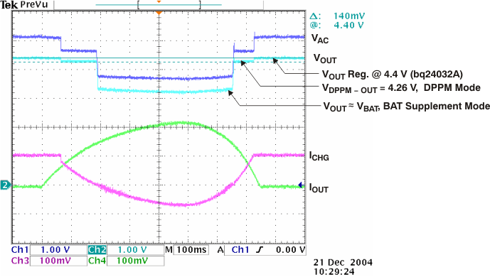 Figure 8. DPPM and Battery Supplement Modes
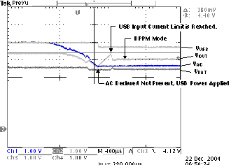 Figure 10. Remove AC – PWR XFER to USB
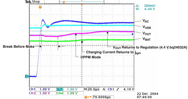
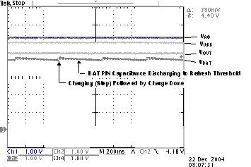 Figure 14. Battery Absent – PWR XFER to USB
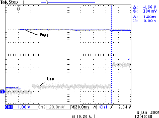 Figure 16. USB Boot-Up Power-Up
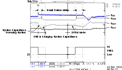 Figure 9. Toggle PSEL Low
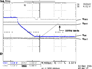 Figure 11. Remove AC (Low Battery) – PWR XFER to USB
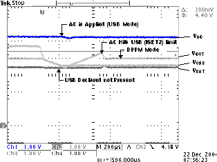 Figure 13. Remove USB – PWR XFER From USB to AC
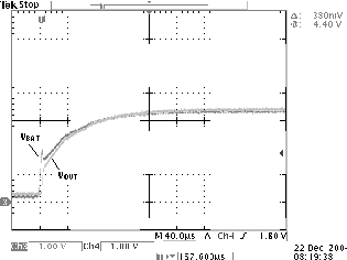 Figure 15. Insert Battery – Power-Up Output via BAT