SLUS618I August   2004  – December 2014

UNLESS OTHERWISE NOTED, this document contains PRODUCTION DATA.  

  1. Features
  2. Applications
  3. Description
  4. Power Flow Diagram
  5. Revision History
  6. Description (continued)
  7. Device Options
  8. Pin Configuration and Functions
  9. Specifications
    1. 9.1 Absolute Maximum Ratings
    2. 9.2 ESD Ratings
    3. 9.3 Recommended Operating Conditions
    4. 9.4 Thermal Information
    5. 9.5 Dissipation Ratings
    6. 9.6 Electrical Characteristics
    7. 9.7 Typical Characteristics
  10. 10Detailed Description
    1. 10.1 Overview
    2. 10.2 Functional Block Diagram
    3. 10.3 Feature Description
      1. 10.3.1  bq24038 Differences
      2. 10.3.2  Power-Path Management
        1. 10.3.2.1 Case 1: AC Mode (PSEL = High)
          1. 10.3.2.1.1 System Power
          2. 10.3.2.1.2 Charge Control
          3. 10.3.2.1.3 Dynamic Power-Path Management (DPPM)
        2. 10.3.2.2 Case 2: USB (PSEL = Low) bq24030/31/32A/38
          1. 10.3.2.2.1 System Power
          2. 10.3.2.2.2 Charge Control
          3. 10.3.2.2.3 Dynamic Power-Path Management (DPPM)
          4. 10.3.2.2.4 Battery Temperature Monitoring
      3. 10.3.3  Charge Status Outputs
      4. 10.3.4  ACPG, USBPG Outputs (Power Good), bq24030/31/32A/35
      5. 10.3.5  PG Output (Power Good), bq24038
      6. 10.3.6  CE Input (Chip Enable)
      7. 10.3.7  VBSEL Input (Battery Voltage Selection), bq24038
      8. 10.3.8  DPPM Used As A Charge Disable Function
      9. 10.3.9  Timer Fault Recovery
      10. 10.3.10 Short-Circuit Recovery
      11. 10.3.11 LDO Regulator
    4. 10.4 Device Functional Modes
      1. 10.4.1 Sleep Mode - V(IN) < VI(BAT)
      2. 10.4.2 Standby Mode - V(IN) > VI(BAT)and CE (Chip Enable) Pin = Low
      3. 10.4.3 Battery Charge Mode - V(IN) > VI(BAT), Battery Present, CE Pin = High and DPPM Pin Not Floating
        1. 10.4.3.1 Autonomous Power Source Selection, PSEL Control Pin
      4. 10.4.4 Charge Control
        1. 10.4.4.1 Battery Pre-Conditioning
        2. 10.4.4.2 Battery Charge Current
        3. 10.4.4.3 Battery Voltage Regulation
        4. 10.4.4.4 Power Handoff
        5. 10.4.4.5 Temperature Regulation and Thermal Protection
        6. 10.4.4.6 Charge Timer Operation
        7. 10.4.4.7 Charge Termination and Recharge
      5. 10.4.5 Boot-Up Sequence
  11. 11Application and Implementation
    1. 11.1 Application Information
    2. 11.2 Typical Application
      1. 11.2.1 Design Requirements
      2. 11.2.2 Detailed Design Procedure
        1. 11.2.2.1 Selecting the Input and Output Capacitors
      3. 11.2.3 Application Curves
  12. 12Power Supply Recommendations
  13. 13Layout
    1. 13.1 Layout Guidelines
    2. 13.2 Layout Example
    3. 13.3 Thermal Considerations
  14. 14Device and Documentation Support
    1. 14.1 Device Support
      1. 14.1.1 Third-Party Products Disclaimer
    2. 14.2 Documentation Support
      1. 14.2.1 Related Documentation
    3. 14.3 Related Links
    4. 14.4 Trademarks
    5. 14.5 Electrostatic Discharge Caution
    6. 14.6 Glossary
  15. 15Mechanical, Packaging, and Orderable Information

封装选项

请参考 PDF 数据表获取器件具体的封装图。

机械数据 (封装 | 引脚)
  • RHL|20
散热焊盘机械数据 (封装 | 引脚)
订购信息

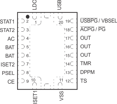
8 Pin Configuration and Functions

RHL Package
20 Pins
Top View
po_lus618.gif

Pin Functions

PIN I/O DESCRIPTION
NAME bq24038 bq24030, 31, 32A, 35
AC 4 4 I Charge input voltage from AC adapter
ACPG 18 O AC power-good status output (open-drain)
BAT 5, 6 5, 6 I/O Battery input and output.
CE 9 9 I Chip enable input (active high)
DPPM 13 13 I Dynamic power-path management set point (account for scale factor)
ISET1 10 10 I/O Charge current set point for AC input and precharge and termination set point for both AC and USB
ISET2 7 7 I Charge current set point for USB port. (High = 500 mA, Low = 100 mA)
LDO 1 1 O 3.3-V LDO regulator
OUT 15, 16, 17 15, 16, 17 O Output terminal to the system
PG 18 O AC or USB power-good status output (open-drain)
PSEL 8 8 I Power source selection input (Low for USB, High for AC)
STAT1 2 2 O Charge status output 1 (open-drain)
STAT2 3 3 O Charge status output 2 (open-drain)
TMR 14 14 I/O Timer program input programmed by resistor. Disable fast-charge safety timer and termination by tying TMR to LDO.
TS 12 12 I/O Temperature sense input
USB 20 20 I USB charge input voltage
USBPG 19 O USB power-good status output (open-drain)
VBSEL 19 I Battery charge voltage selection
VSS 11 11 Ground input (the thermal pad on the underside of the package) There is an internal electrical connection between the exposed thermal pad and VSS pin of the device. The exposed thermal pad must be connected to the same potential as the VSS pin on the printed-circuit board. Do not use the thermal pad as the primary ground input for the device. VSS pin must be connected to ground at all times.