SLUS618I August 2004 – December 2014
UNLESS OTHERWISE NOTED, this document contains PRODUCTION DATA.
- 1 Features
- 2 Applications
- 3 Description
- 4 Power Flow Diagram
- 5 Revision History
- 6 Description (continued)
- 7 Device Options
- 8 Pin Configuration and Functions
- 9 Specifications
-
10Detailed Description
- 10.1 Overview
- 10.2 Functional Block Diagram
- 10.3
Feature Description
- 10.3.1 bq24038 Differences
- 10.3.2 Power-Path Management
- 10.3.3 Charge Status Outputs
- 10.3.4 ACPG, USBPG Outputs (Power Good), bq24030/31/32A/35
- 10.3.5 PG Output (Power Good), bq24038
- 10.3.6 CE Input (Chip Enable)
- 10.3.7 VBSEL Input (Battery Voltage Selection), bq24038
- 10.3.8 DPPM Used As A Charge Disable Function
- 10.3.9 Timer Fault Recovery
- 10.3.10 Short-Circuit Recovery
- 10.3.11 LDO Regulator
- 10.4 Device Functional Modes
- 11Application and Implementation
- 12Power Supply Recommendations
- 13Layout
- 14Device and Documentation Support
- 15Mechanical, Packaging, and Orderable Information
封装选项
请参考 PDF 数据表获取器件具体的封装图。
机械数据 (封装 | 引脚)
- RHL|20
散热焊盘机械数据 (封装 | 引脚)
- RHL|20
订购信息
10 Detailed Description
10.1 Overview
The bqTINY III-series of devices are highly integrated Li-ion linear chargers and system power-path management devices targeted at space-limited portable applications. The bqTINY III-series offer integrated USB-port and DC supply (AC adapter), power-path management with autonomous power-source selection, power FETs and current sensors, high accuracy current and voltage regulation, charge status, and charge termination, in a single monolithic device.
The bqTINY III-series supports a precision Li-ion or Li-polymer charging system suitable for single-cell portable devices. See a typical charge profile, application circuit, and an operational flow chart in Figure 2 through Figure 6, respectively.
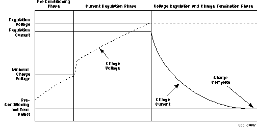 Figure 2. Charge Profile
The bqTINY III-series power the system while independently charging the battery. This feature reduces the charge and discharge cycles on the battery, allows for proper charge termination and allows the system to run with an absent or defective battery pack. This feature also allows for the system to instantaneously turn on from an external power source in the case of a deeply discharged battery pack. The IC design is focused on supplying continuous power to the system when available from the AC adapter, USB port or battery sources.
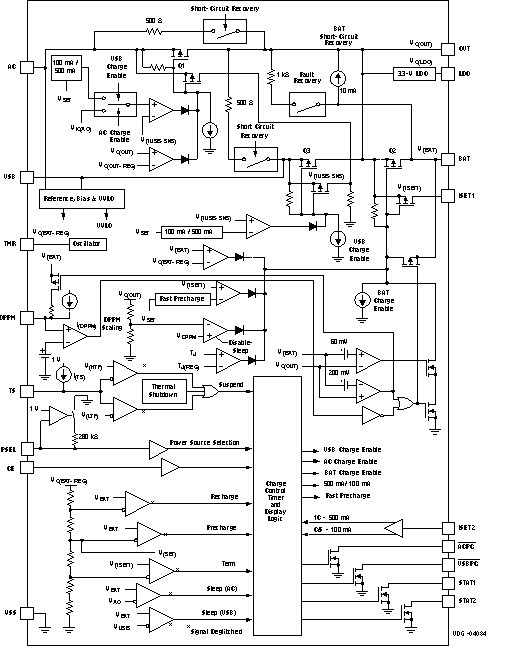
10.2 Functional Block Diagram1
10.3 Feature Description
10.3.1 bq24038 Differences
The bq24038 replaces USBPG with pin VBSEL, to enable user selection of the charge voltage. In addition, pin ACPG was modified to PG. PG is active low when either AC power or USB power is detected.
10.3.2 Power-Path Management
The bqTINY III-series powers the system while independently charging the battery. This features reduces the charge and discharge cycles on the battery, allows for proper charge termination, and allows the system to run with an absent or defective battery pack. This feature gives the system priority on input power, allowing the system to power up with a deeply discharged battery pack. This feature works as follows (note that PSEL is assumed HIGH for this discussion).
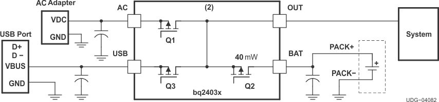 Figure 3. Power-Path Management
10.3.2.1 Case 1: AC Mode (PSEL = High)
10.3.2.1.1 System Power
In this case, the system load is powered directly from the AC adapter through the internal transistor Q1 (see Figure 3). For bq24030/31, Q1 acts as a switch as long as the AC input remains at or below 6 V (VO(OUT-REG)). Once the AC voltage goes above 6 V, Q1 starts regulating the output voltage at 6 V. For bq24035, once the AC voltage goes above VCUT-OFF (~6.4 V), Q1 turns off. For bq24032A/38, the output is regulated at 4.4 V from the AC input. Note that switch Q3 is turned off for both devices. If the system load exceeds the capacity of the supply, the output voltage drops down to the battery's voltage.
10.3.2.1.2 Charge Control
When AC is present, the battery is charged through switch Q2 based on the charge rate set on the ISET1 input.
10.3.2.1.3 Dynamic Power-Path Management (DPPM)
This feature monitors the output voltage (system voltage) for input power loss due to brown outs, current limiting, or removal of the input supply. If the voltage on the OUT pin drops to a preset value, V(DPPM-SET) × SF, due to a limited amount of input current, then the battery charging current is reduced until the output voltage stops dropping. The DPPM control tries to reach a steady-state condition where the system gets its needed current and the battery is charged with the remaining current. No active control limits the current to the system; therefore, if the system demands more current than the input can provide, the output voltage drops just below the battery voltage and Q2 turns on which supplements the input current to the system. DPPM has three main advantages.
- This feature allows the designer to select a lower power wall adapter, if the average system load is moderate compared to its peak power. For example, if the peak system load is 1.75 A, average system load is 0.5 A and battery fast-charge current is 1.25 A, the total peak demand could be 3 A. With DPPM, a 2-A adaptor could be selected instead of a 3.25-A supply. During the system peak load of 1.75 A and charge load of 1.25 A, the smaller adaptor’s voltage drops until the output voltage reaches the DPPM regulation voltage threshold. The charge current is reduced until there is no further drop on the output voltage. The system gets its 1.75-A charge and the battery charge current is reduced from 1.25 A to 0.25 A. When the peak system load drops to 0.5 A, the charge current returns to 1 A and the output voltage returns to its normal value.
- Using DPPM provides a power savings compared to configurations without DPPM. Without DPPM, if the system current plus charge current exceed the supply’s current limit, then the output is pulled down to the battery. Linear chargers dissipate the unused power (VIN-VOUT) × ILOAD. The current remains high (at current limit) and the voltage drop is large for maximum power dissipation. With DPPM, the voltage drop is less (VIN-V(DPPM-REG)) to the system which means better efficiency. The efficiency for charging the battery is the same for both cases. The advantages include less power dissipation, lower system temperature, and better overall efficiency.
- The DPPM sustains the system voltage no matter what causes it to drop, if at all possible. It does this by reducing the noncritical charging load while maintaining the maximum power output of the adaptor.
Note that the DPPM voltage, V(DPPM-REG), is programmed as follows:

where
- R(DPPM) is the external resistor connected between the DPPM and VSS pins.
- I(DPPM) is the internal current source.
- SF is the scale factor as specified in the specification table.
The safety timer is dynamically adjusted while in DPPM mode. The voltage on the ISET1 pin is directly proportional to the programmed charging current. When the programmed charging current is reduced, due to DPPM, the ISET1 and TMR voltages are reduced and the timer’s clock is proportionally slowed, extending the safety time. In normal operation, V(TMR) = 2.5 V; when the clock is slowed the voltage V(TMR) is reduced. For example, if V(TMR) = 1.25 V, the safety timer has a value close to 2 times the normal operation timer value. See Figure 8 through Figure 11.
10.3.2.2 Case 2: USB (PSEL = Low) bq24030/31/32A/38
10.3.2.2.1 System Power
In this case, the system load is powered directly from the USB port through the internal switch Q3 (see Figure 4). Note in this case, Q3 regulates the total current to the 100 mA or 500 mA level, as selected on the ISET2 input. Switch Q1 is turned off in this mode. If the system and battery load is less than the selected regulated limit, then Q3 is fully on and VOUT is approximately (V(USB)-V(USB-DO)). The systems power management is responsible for keeping its system load below the USB current level selected (if the battery is critically low or missing). Otherwise, the output drops to the battery voltage; therefore, the system should have a low power mode for USB power application. The DPPM feature keeps the output from dropping below its programmed threshold, due to the battery charging current, by reducing the charging current.
10.3.2.2.2 Charge Control
When USB is present and selected, Q3 regulates the input current to the value selected by the ISET2 pin (0.1/0.5 A). The charge current to the battery is set by the ISET1 resistor (typically > 0.5 A). Because the charge current typically is programmed for more current than Q3 allows, the output voltage drops to the battery voltage or DPPM voltage, whichever is higher. If the DPPM threshold is reached first, the charge current is reduced until VOUT stops dropping. If VOUT drops to the battery voltage, the battery is able to supplement the input current to the system.
10.3.2.2.3 Dynamic Power-Path Management (DPPM)
The theory of operation is the same as described in CASE 1, except that Q3 restricts the amount of input current delivered to the output and battery instead of the input supply.
Note that the DPPM voltage, V(DPPM), is programmed as follows:
and

where
- R(DPPM) is the external resistor connected between the DPPM and VSS pins.
- I(DPPM) is the internal current source.
- SF is the scale factor as specified in the specification table.
10.3.2.2.4 Battery Temperature Monitoring
The bqTINY™ III-series continuously monitors battery temperature by measuring the voltage between the TS and VSS pins. An internal current source (I(TS) = 100 μA, typical) provides the bias for most common 10-kΩ negative-temperature coefficient thermistors (NTC) (see Figure 4). The device compares the voltage on the TS pin against the internal V(LTF) , and V(HTF) thresholds (0.5 V and 2.5 V, respectively are typical) to determine if charging is allowed. Once a temperature outside the V(LTF) and V(HTF) thresholds is detected, the device immediately suspends the charge. The device suspends charge by turning off the power FET and holding the timer value (i.e., timers are not reset). Charge is resumed when the temperature returns to the normal range. The allowed temperature range for 103AT-type thermistor is 0°C to 45°C. However, the user may increase the range by adding two external resistors. See Figure 5.
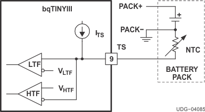 Figure 4. TS Pin Configuration
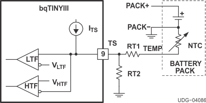 Figure 5. TS Pin Thresholds
10.3.3 Charge Status Outputs
The open-drain (OD) STAT1 and STAT2 outputs indicate various charger operations as shown in Table 1. These status pins can be used to drive LEDs or communicate to the host processor. Note that OFF indicates the open-drain transistor is turned off. Note that this assumes CE = High.
Table 1. Status Pins Summary
| CHARGE STATE | STAT1 | STAT2 |
|---|---|---|
| Precharge in progress | ON | ON |
| Fast charge in progress | ON | OFF |
| Charge done | OFF | ON |
| Charge suspend (temperature), timer fault, and sleep mode | OFF | OFF |
10.3.4 ACPG, USBPG Outputs (Power Good), bq24030/31/32A/35
The two open-drain pins, ACPG, USBPG (AC and USB power good), indicate when the AC adapter or USB port is present and above the battery voltage. The corresponding output turns ON (low) when exiting sleep mode (input voltage above battery voltage). This output is turned off in the sleep mode (open drain). The ACPG, USBPG pins can be used to drive an LED or communicate to the host processor. Note that OFF indicates the open-drain transistor is turned off.
10.3.5 PG Output (Power Good), bq24038
The open-drain pin PG indicates when either the AC adapter or USB port is present and above the battery voltage. This output is turned off in sleep mode (open drain). The PG pin can be used to drive a LED or communicate with the host processor.
10.3.6 CE Input (Chip Enable)
The CE (chip enable) digital input is used to disable or enable the bqTINY III-series. A high-level signal on this pin enables the chip, and a low-level signal disables the device and initiates the standby mode. The bqTINY III-series enters the low-power standby mode when the CE input is low with either AC or USB present. In this suspend mode, internal power FETs Q1 and Q3 (see Figure 3) are turned off; the battery (BAT pin) is used to power the system via Q2 and the OUT pin which also powers the LDO. This feature is designed to limit the power drawn from the input supplies (such as USB suspend mode).
10.3.7 VBSEL Input (Battery Voltage Selection), bq24038
The VBSEL (battery voltage select) digital input pin can be used to set the charge voltage to 4.2 V typical (VBSEL = low) or 4.36 V typical (VBSEL = high). If VBSEL is left open, an internal current source pulldown ensures that the charge voltage is set to 4.2 V typical.
10.3.8 DPPM Used As A Charge Disable Function
The DPPM pin can be used to disable the charge process. The DPPM pin has an output current source that, when used with a resistor, sets the DPPM threshold. If the chosen resistance is too high, then the "DPPM-OUT" voltage is programmed higher than the OUT pin regulation voltage and the part is put in DPPM mode. In this mode the charging current is reduced until the OUT pin recovers to the DPPM_OUT threshold. Since the OUT pin is in voltage regulation (below the DPPM-OUT threshold) it does not increase in amplitude, and the charge current turns completely off. In DPPM mode the charge termination is diabled.
Note that the OUT pin regulates at 4.4V ±0.1V, with an adaptor input, on the bq24032A/bq24038 ICs, is switched straight through on the bq24030/5 ICs (up to 6V); and, on USB inputs (all ICs) is switched straight through from the USB input to the OUT pin.
If the DPPM pin is floated (resistor disconnected) then the DPPM pin will be driven high and the charge current will go to zero. Note that this applies to both AC and USB charging. Another way to disable the charging is to externally drive the DPPM pin high (to the OUT pin voltage).
10.3.9 Timer Fault Recovery
As shown in Figure 6, bqTINY III-series provides a recovery method to deal with timer fault conditions. The following summarizes this method:
Condition 1: Charge voltage above recharge threshold (V(RCH)) and timeout fault occurs.
Recovery Method: bqTINY III-series waits for the battery voltage to fall below the recharge threshold. This could happen as a result of a load on the battery, self-discharge, or battery removal. Once the battery falls below the recharge threshold, the bqTINY III-series clears the fault and starts a new charge cycle. A POR or CE toggle also clears the fault.
Condition 2: Charge voltage below recharge threshold (V(RCH)) and timeout fault occurs.
Recovery Method: Under this scenario, the bqTINY III-series applies the I(FAULT) current. This small current is used to detect a battery removal condition and remains on as long as the battery voltage stays below the recharge threshold. If the battery voltage goes above the recharge threshold, then the bqTINY III-series disables the I(FAULT) current and executes the recovery method described for condition 1. Once the battery falls below the recharge threshold, the bqTINY III-series clears the fault and starts a new charge cycle. A POR or CE toggle also clears the fault.
10.3.10 Short-Circuit Recovery
The output can experience two types of short-circuit protection, one associated with the input and one with the battery.
If the output drops below ~1 V, an output short-circuit condition is declared and the input FETs (AC and USB) are turned off. To recover from this state, a 500-Ω pullup resistor from each input is applied (switched) to the output. To recover, the load on the output has to be reduced {Rload > 1 V × 500 Ω/ (Vin–Vout)} such that the pullup resistor is able to lift the output voltage above 1 V, for the input FETs to be turned back on.
If the output drops 200 mV below the battery voltage, the battery FET is considered in short circuit and the battery FET turns off. To recover from this state, there is a 10-mA ±8 mA current source from the battery to the output. Once the output load is reduced, such that the current source can pick up the output within 200 mV of the battery, the FET turns back on (As Vout increases in voltage the current source's drive drops toward 2 mA).
If the short is removed, and the minimum system load is still too large [R<(VBat –200 mV / 2mA)], the short-circuit protection can be temporarily defeated. The battery short-circuit protection can be disabled (recommended only for a short time) if the voltage on the DPPM pin is less than 1 V. Pulsing this pin below 1 V, for a few microseconds, should be enough to recover.
This short-circuit disable feature was implemented mainly for power up when inserting a battery. Because the BAT input voltage rises much faster than the OUT voltage (Vout<Vbat-200 mV), with most any capacitive load on the output, the part can get stuck in short-circuit mode. Placing a capacitor between the DPPM pin and ground slows the VDPPM rise time, during power up, and delays the short-circuit protection. Too large a capacitance on this pin (too much of a delay) could allow too-high currents if the output was shorted to ground. The recommended capacitance is 1 nF to 10 nF. The VDPPM rise time is a function of the 100-µA DPPM current source, the DPPM resistor, and the capacitor added.
10.3.11 LDO Regulator
The bqTINY III-series provides a 3.3-V LDO regulator. This regulator is typically used to power USB transceiver or drivers in portable applications. Note that this LDO is only enabled when either AC or USB inputs are present. If the CE pin is low (chip disabled) and AC or USB is present, the LDO is powered by the battery. This is to ensure low input current when the chip is disabled.
10.4 Device Functional Modes
10.4.1 Sleep Mode - V(IN) < VI(BAT)
The bqTINY III-series charger circuitry enters the low-power sleep mode if both AC and USB are removed from the circuit. This feature prevents draining the battery into the bqTINY III-series during the absence of input supplies. Note that in sleep mode, Q2 remains on (i.e., battery connected to the OUT pin) in order for the battery to continue supplying power to the system.
The bqTINY III-series enters the low-power standby mode if while AC or USB is present, the CE input is low. In this suspend mode, internal power FETs Q1 and Q3 (see Figure 3) are turned off, the BAT input is used to power the system through OUT pin, and the LDO remains on (powered from output). This feature is designed to limit the power drawn from the input supplies (such as USB suspend mode).
10.4.2 Standby Mode - V(IN) > VI(BAT)and CE (Chip Enable) Pin = Low
The CE (chip enable) digital input is used to disable or enable the IC. A high-level signal on this pin enables the chip, and a low-level signal disables the device and initiates the standby mode. The bqTINY III-series enters the low-power standby mode when the CE input is low with input present. In this suspend mode, internal power FETs Q1 and Q3 (see Figure 3) are turned off, the BAT input is used to power the system through OUT pin, and the LDO remains on (powered from output). This feature is designed to limit the power drawn from the input supplies (such as USB suspend mode).
10.4.3 Battery Charge Mode - V(IN) > VI(BAT), Battery Present, CE Pin = High and DPPM Pin Not Floating
10.4.3.1 Autonomous Power Source Selection, PSEL Control Pin
The PSEL pin selects the priority of the input sources (high = AC, low = USB), if that primary source is not available (based on ACPG, USBPG signal), then it uses the secondary source. If neither input source is available, then the battery is selected as the source. With the PSEL input high, the bqTINY III-series attempts to charge from the AC input. If AC input is not present, the USB is selected. If both inputs are available, the AC adapter has priority. With the PSEL input low, the bqTINY III-series defaults to USB charging. If USB input is grounded, then the bqTINY III-series charges from the AC input at the USB charge rate (as selected by ISET2). This feature can be used in system where AC and USB power source selection is done elsewhere. The PSEL function is summarized in Table 2.
Table 2. Power Source Selection Function Summary
| PSEL STATE | AC | USB | CHARGE SOURCE |
MAXIMUM CHARGE RATE(1) |
SYSTEM POWER SOURCE | USB BOOT-UP FEATURE |
|---|---|---|---|---|---|---|
| Low | Present(2) | Absent | AC | ISET2 | AC | Enabled |
| Absent(3) | Present | USB | ISET2 | USB | Enabled | |
| Present | Present | USB | ISET2 | USB | Enabled | |
| Absent | Absent | N/A | N/A | Battery | Disabled | |
| High | Present | Absent | AC | ISET1 | AC | Disabled |
| Absent | Present | USB | ISET2 | USB | Disabled | |
| Present | Present | AC | ISET1 | AC | Disabled | |
| Absent | Absent | N/A | N/A | Battery | Disabled |
10.4.4 Charge Control
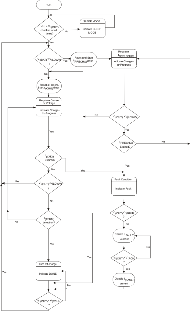 Figure 6. Charge Control Operational Flow Chart
10.4.4.1 Battery Pre-Conditioning
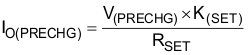
During a charge cycle, if the battery voltage is below the V(LOWV) threshold (3.0 V, typical), the bqTINY III-series applies a precharge current, IO(PRECHG), to the battery. This feature revives deeply discharged cells. The resistor connected between the ISET1 and VSS, RSET, determines the precharge rate. The V(PRECHG) and K(SET) parameters are specified in the specifications table. Note that this applies to both AC and USB charging.
The bqTINY III-series activates a safety timer, t(PRECHG), during the conditioning phase. If V(LOWV) threshold is not reached within the timer period, the bqTINY III-series turns off the charger and enunciates FAULT on the STAT1 and STAT2 pins. The timeout is extended if the charge current is reduced by DPPM. See the Timer Fault Recovery section for additional details.
10.4.4.2 Battery Charge Current
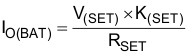
The bqTINY III-series offers on-chip current regulation with programmable set point. The resistor connected between the ISET1 and VSS, RSET, determines the charge level. The charge level may be reduced to give the system priority on input current (see DPPM). The V(SET) and K(SET) parameters are specified in the specifications table.
When powered from a USB port, the input current available (0.1 A/0.5 A) is typically less than the programmed (ISET1) charging current, and therefore, the DPPM feature attempts to keep the output from being pulled down by reducing the charging current.
The charge level for the bq24032A/38, during AC operation only (PSEL = High), can be changed by a factor of 2 by setting the ISET2 pin high (full charge) or low (half charge). The voltage on the ISET1 pin, V(SET), is divided by 2 when in the half constant current charge mode. Note that with PSEL low, the ISET2 pin controls only the 0.1 A/0.5 A USB current level.
With ISET2 low the V(TMR) voltage remains at 2.5 V under normal operating conditions. In this case, the charge rate is half the programmed current but the safety timer remains t(CHG). If the bqTINY III-series enters DPPM or thermal regulation mode from this state, the safety timer immediately doubles and then the safety time is adjusted (inversely proportionate) with the charge current.
See the section titled Power-Path Management for additional details.
10.4.4.3 Battery Voltage Regulation
The voltage regulation feedback is through the BAT pin. This input is tied directly to the positive side of the battery pack. The bqTINY III-series monitors the battery-pack voltage between the BAT and VSS pins. When the battery voltage rises to the VO(BAT-REG) threshold (4.1-V, 4.2-V, or 4.36-V versions), the voltage regulation phase begins and the charging current begins to taper down.
If the battery is absent, the BAT pin cycles between charge done (VO(REG)) and charging (battery refresh threshold, ~100 mV below VO(REG)). See Figure 14.
See Figure 15 for power up by battery insertion.
As a safety backup, the bqTINY III-series also monitors the charge time in the charge mode. If charge is not terminated within this time period, t(CHG), the bqTINY III-series turns off the charger and enunciates FAULT on the STAT1 and STAT2 pins. See the DPPM operation under Case 1 for information on extending the safety timer during DPPM operation. See theTimer Fault Recovery section for additional details.
10.4.4.4 Power Handoff
The design goal of the bqTINY III-series is to keep the system powered at all times (OUT pin); first, by either AC or USB input––priority chosen by PSEL, and lastly by the battery. The input power source is only considered present if its power-good status is low. There is a break-before-make switching action when switching between AC to USB or USB to AC, for tSW-AC/USB, where the system capacitance should hold up the system voltage. Note that the transfer of power occurs when the sources power-good pin goes high (open-drain output high = power not present), which is when the input source drops to the battery's voltage. If the battery is below a useable voltage, the system may reset. Typically, prior to losing the input power, the battery would have some useable capacity, and a system reset would be avoided. If the battery was dead or missing, the system would lose power unless the PSEL pin was used to transfer power prior to shutdown.
If this is a concern, there is a simple external solution. Externally toggling the PSEL (bq24030/31/5/8) pin immediately starts the power-transfer process (does not wait for input to drop to the battery's voltage). This can be implemented by a resistor divider between the AC input and ground with the PSEL pin tied between R1 (top resistor) and R2 (resistor to ground). The resistor values are chosen such that the divider voltage will be at 1 V (PSEL threshold) when the AC has dropped to its critical voltage (user defined). An internal ~280-kΩ resistor is applied when PSEL < 1 V, to provide hysteresis. Choose R2 between 10 kΩ and 60 kΩ and V(ac-critical) between 3.5 V and 4.5 V. R1 can be found using the following equation:
Example: If R2 = 30 kΩ and V(ac-critical) = 4 V; R1 = 30 kΩ(4 V – 1 V) = 90 kΩ, V(ac-reset) = 1+ 90k (30 k+280 k)/(280 k×30 k) = 4.32 V. Therefore, for a 90 kΩ/30 kΩ divider, the bias on PSEL would switch power from AC to USB (USBPG = L) when the VAC dropped to 4 V (independent of VBAT) and switches back when the VAC recovers to 4.32 V. See Figure 9 through Figure 13.
10.4.4.5 Temperature Regulation and Thermal Protection
In order to maximize charge rate, the bqTINY III-series features a junction temperature regulation loop. If the power dissipation of the bqTINY III-series results in a junction temperature greater than the TJ(REG) threshold (125°C, typical), the bqTINY III-series throttles back on the charge current in order to maintain a junction temperature around the TJ(REG) threshold. To avoid false termination, the termination detect function is disabled while in this mode. The reduced charge current results in a longer charge time so the safety timer, t(CHG) is extended inversely. This means that if the temperature regulation loop reduces the current to half of the programmed charge rate, then the safety timer t(CHG) doubles. See Charge Timer Operation for more detail.
The bqTINY III-series also monitors the junction temperature, TJ, of the die and disconnects the OUT pin from AC or USB inputs if TJ exceeds T(SHTDWN). This operation continues until TJ falls below T(SHTDWN) by the hysteresis level specified in the specification table.
The battery supplement mode has no thermal protection. The Q2 FET continues to connect the battery to the output (system), if input power is not sufficient; however, a short-circuit protection circuit limits the battery discharge current such that the maximum power dissipation of the part is not exceeded under typical design conditions.
10.4.4.6 Charge Timer Operation
As a safety backup, the bqTINY III-series monitors the charge time in the charge mode. If the termination threshold is not detected within the time period, t(CHG), the bqTINY III-series turns off the charger and enunciates FAULT on the STAT1 and STAT2 pins. The resistor connected between the TMR and VSS, RTMR, determines the timer period. The K(TMR) parameter is specified in the specifications table. In order to disable the charge timer, eliminate RTMR, connect the TMR pin directly to the LDO pin. Note that this action eliminates the fast-charge safety timer (it does not disable or reset the pre-charge safety timer), disables termination, and also clears a fast-charge timer fault. TMR pin should not be left floating.
While in the thermal regulation mode or DPPM mode, the bqTINY III-series dynamically adjusts the timer period in order to provide the additional time needed to fully charge the battery. This proprietary feature is designed to prevent against early or false termination. The maximum charge time in this mode, t(CHG-TREG), is calculated by Equation 8.
Note that because this adjustment is dynamic and changes as the ambient temperature changes and the charge level changes, the timer clock is adjusted. It is difficult to estimate a total safety time without integrating the above equation over the charge cycle. Therefore, understanding the theory that the safety time is adjusted inversely proportionately with the charge current and the battery is a current-hour rating, the safety time dynamically adjusts appropriately.
The V(SET) parameter is specified in the specifications table. V(SET-TREG) is the voltage on the ISET pin during the thermal regulation or DPPM mode and is a function of charge current. (Note that charge current is dynamically adjusted during the thermal regulation or DPPM mode.)
All deglitch times also adjusted proportionally to t(CHG-TREG).
10.4.4.7 Charge Termination and Recharge
The bqTINY III-series monitors the voltage on the ISET1 pin, during voltage regulation, to determine when termination should occur (C/10 – 250 mV, C/25 – 100 mV). Once the termination threshold, I(TERM), is detected the bqTINY III-series terminates charge. The resistor connected between the ISET1 and VSS, RSET, programs the fast charge current level (C level, VISET1 = 2.5 V) and thus the C/10 and C/25 current termination threshold levels. The V(TERM) and K(SET) parameters are specified in the specifications table. Note that this applies to both AC and USB charging.

After charge termination, the bqTINY III-series re-starts the charge once the voltage on the OUT pin falls below the V(RCH) threshold (VO(BAT-REG) –100 mV, typical). This feature keeps the battery at full capacity at all times.
10.4.5 Boot-Up Sequence
In order to facilitate the system start-up and USB enumeration, the bqTINY III-series offers a proprietary boot-up sequence. On the first application of power to the bqTINY III-series, this feature enables the 100-mA USB charge rate for a period of approximately 150 ms, (t(BOOT-UP)), ignoring the ISET2 and CE inputs setting. At the end of this period, the bqTINY III-series implements CE and ISET2 inputs settings. Table 2 indicates when this feature is enabled. See Figure 16.