SLUS618I August 2004 – December 2014
UNLESS OTHERWISE NOTED, this document contains PRODUCTION DATA.
- 1 Features
- 2 Applications
- 3 Description
- 4 Power Flow Diagram
- 5 Revision History
- 6 Description (continued)
- 7 Device Options
- 8 Pin Configuration and Functions
- 9 Specifications
-
10Detailed Description
- 10.1 Overview
- 10.2 Functional Block Diagram
- 10.3
Feature Description
- 10.3.1 bq24038 Differences
- 10.3.2 Power-Path Management
- 10.3.3 Charge Status Outputs
- 10.3.4 ACPG, USBPG Outputs (Power Good), bq24030/31/32A/35
- 10.3.5 PG Output (Power Good), bq24038
- 10.3.6 CE Input (Chip Enable)
- 10.3.7 VBSEL Input (Battery Voltage Selection), bq24038
- 10.3.8 DPPM Used As A Charge Disable Function
- 10.3.9 Timer Fault Recovery
- 10.3.10 Short-Circuit Recovery
- 10.3.11 LDO Regulator
- 10.4 Device Functional Modes
- 11Application and Implementation
- 12Power Supply Recommendations
- 13Layout
- 14Device and Documentation Support
- 15Mechanical, Packaging, and Orderable Information
封装选项
请参考 PDF 数据表获取器件具体的封装图。
机械数据 (封装 | 引脚)
- RHL|20
散热焊盘机械数据 (封装 | 引脚)
- RHL|20
订购信息
13 Layout
13.1 Layout Guidelines
It is important to pay special attention to the PCB layout. The following provides some guidelines:
- To obtain optimal performance, the decoupling capacitor from input terminals to VSS and the output filter capacitors from OUT to VSS should be placed as close as possible to the bqTINY III-series, with short trace runs to both signal and VSS pins.
- All low-current VSS connections should be kept separate from the high-current charge or discharge paths from the battery. Use a single-point ground technique incorporating both the small signal ground path and the power ground path.
- The high-current charge paths into AC and USB and from the BAT and OUT pins must be sized appropriately for the maximum charge current in order to avoid voltage drops in these traces.
- The bqTINY III-series is packaged in a thermally enhanced MLP package. The package includes a QFN thermal pad to provide an effective thermal contact between the device and the printed-circuit board. Full PCB design guidelines for this package are provided in the application note entitled QFN/SON PCB Attachment (SLUA271).
13.2 Layout Example
 Figure 17. Layout Schematic
13.3 Thermal Considerations
The bqTINY III-series is packaged in a thermally enhanced MLP package. The package includes a QFN thermal pad to provide an effective thermal contact between the device and the printed-circuit board (PCB). Full PCB design guidelines for this package are provided in the application note entitled QFN/SON PCB Attachment (SLUA271). The power pad should be tied to the VSS plane. The most common measure of package thermal performance is thermal impedance (θJA) measured (or modeled) from the chip junction to the air surrounding the package surface (ambient).
The mathematical expression for θJA is:
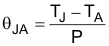
where
- TJ = chip junction temperature
- TA = ambient temperature
- P = device power dissipation
Factors that can greatly influence the measurement and calculation of θJA include:
- whether or not the device is board mounted
- trace size, composition, thickness, and geometry
- orientation of the device (horizontal or vertical)
- volume of the ambient air surrounding the device under test and airflow
- whether other surfaces are in close proximity to the device being tested
The device power dissipation, P, is a function of the charge rate and the voltage drop across the internal power FET. It can be calculated from Equation 12:

Due to the charge profile of Li-xx batteries, the maximum power dissipation is typically seen at the beginning of the charge cycle when the battery voltage is at its lowest. See Figure 2. Typically the Li-ion battery's voltage quickly (< 2 V minutes) ramps to approximately 3.5 V, when entering fast charge (1-C charge rate and battery above V(LOWV)). Therefore, it is customary to perform the steady-state thermal design using 3.5 V as the minimum battery voltage because the system board and charging device does not have time to reach a maximum temperature due to the thermal mass of the assembly during the early stages of fast charge. This theory is easily verified by performing a charge cycle on a discharged battery while monitoring the battery voltage and chargers power pad temperature.