ZHCSNQ2C March   2021  – January 2024 AWR1843AOP

PRODUCTION DATA  

  1.   1
  2. 特性
  3. 应用
  4. 说明
    1. 3.1 功能方框图
  5. Device Comparison
    1. 4.1 Related Products
  6. Terminal Configuration and Functions
    1. 5.1 Pin Diagram
    2. 5.2 Pin Attributes
    3. 5.3 Signal Descriptions
      1. 5.3.1 Pin Functions - Digital and Analog [ALP Package]
  7. Specifications
    1. 6.1  Absolute Maximum Ratings
    2. 6.2  ESD Ratings
    3. 6.3  Power-On Hours (POH)
    4. 6.4  Recommended Operating Conditions
    5. 6.5  Power Supply Specifications
    6. 6.6  Power Consumption Summary
    7. 6.7  RF Specification
    8. 6.8  CPU Specifications
    9. 6.9  Thermal Resistance Characteristics for FCBGA Package [ALP0180A]
    10. 6.10 Timing and Switching Characteristics
      1. 6.10.1  Antenna Radiation Patterns
        1. 6.10.1.1 Antenna Radiation Patterns for Receiver
        2. 6.10.1.2 Antenna Radiation Patterns for Transmitter
      2. 6.10.2  Antenna Positions
      3. 6.10.3  Power Supply Sequencing and Reset Timing
      4. 6.10.4  Input Clocks and Oscillators
        1. 6.10.4.1 Clock Specifications
      5. 6.10.5  Multibuffered / Standard Serial Peripheral Interface (MibSPI)
        1. 6.10.5.1 Peripheral Description
        2. 6.10.5.2 MibSPI Transmit and Receive RAM Organization
          1. 6.10.5.2.1 SPI Timing Conditions
          2. 6.10.5.2.2 SPI Controller Mode Switching Parameters (CLOCK PHASE = 0, SPICLK = output, SPISIMO = output, and SPISOMI = input)
          3. 6.10.5.2.3 SPI Controller Mode Switching Parameters (CLOCK PHASE = 1, SPICLK = output, SPISIMO = output, and SPISOMI = input)
        3. 6.10.5.3 SPI Peripheral Mode I/O Timings
          1. 6.10.5.3.1 SPI Peripheral Mode Switching Parameters (SPICLK = input, SPISIMO = input, and SPISOMI = output)
        4. 6.10.5.4 Typical Interface Protocol Diagram (Slave Mode)
      6. 6.10.6  LVDS Interface Configuration
        1. 6.10.6.1 LVDS Interface Timings
      7. 6.10.7  General-Purpose Input/Output
        1. 6.10.7.1 Switching Characteristics for Output Timing versus Load Capacitance (CL) #GUID-4685AB93-A014-47EA-9F05-952FFC28DBFA/T4362547-45 #GUID-4685AB93-A014-47EA-9F05-952FFC28DBFA/T4362547-50
      8. 6.10.8  Controller Area Network Interface (DCAN)
        1. 6.10.8.1 Dynamic Characteristics for the DCANx TX and RX Pins
      9. 6.10.9  Controller Area Network - Flexible Data-rate (CAN-FD)
        1. 6.10.9.1 Dynamic Characteristics for the CANx TX and RX Pins
      10. 6.10.10 Serial Communication Interface (SCI)
        1. 6.10.10.1 SCI Timing Requirements
      11. 6.10.11 Inter-Integrated Circuit Interface (I2C)
        1. 6.10.11.1 I2C Timing Requirements #GUID-64613E7E-5DDF-4B01-8FA0-13739060F368/T4362547-185
      12. 6.10.12 Quad Serial Peripheral Interface (QSPI)
        1. 6.10.12.1 QSPI Timing Conditions
        2. 6.10.12.2 Timing Requirements for QSPI Input (Read) Timings #GUID-6A95C194-2C40-46FE-9793-4574200DA2C4/T4362547-210 #GUID-6A95C194-2C40-46FE-9793-4574200DA2C4/T4362547-209
        3. 6.10.12.3 QSPI Switching Characteristics
      13. 6.10.13 ETM Trace Interface
        1. 6.10.13.1 ETMTRACE Timing Conditions
        2. 6.10.13.2 ETM TRACE Switching Characteristics
      14. 6.10.14 Data Modification Module (DMM)
        1. 6.10.14.1 DMM Timing Requirements
      15. 6.10.15 JTAG Interface
        1. 6.10.15.1 JTAG Timing Conditions
        2. 6.10.15.2 Timing Requirements for IEEE 1149.1 JTAG
        3. 6.10.15.3 Switching Characteristics Over Recommended Operating Conditions for IEEE 1149.1 JTAG
  8. Detailed Description
    1. 7.1 Overview
    2. 7.2 Functional Block Diagram
    3. 7.3 Subsystems
      1. 7.3.1 RF and Analog Subsystem
        1. 7.3.1.1 Clock Subsystem
        2. 7.3.1.2 Transmit Subsystem
        3. 7.3.1.3 Receive Subsystem
      2. 7.3.2 Processor Subsystem
      3. 7.3.3 Automotive Interface
      4. 7.3.4 Main Subsystem Cortex-R4F Memory Map
      5. 7.3.5 DSP Subsystem Memory Map
    4. 7.4 Other Subsystems
      1. 7.4.1 ADC Channels (Service) for User Application
        1. 7.4.1.1 GP-ADC Parameter
  9. Monitoring and Diagnostics
    1. 8.1 Monitoring and Diagnostic Mechanisms
      1. 8.1.1 Error Signaling Module
  10. Applications, Implementation, and Layout
    1. 9.1 Application Information
    2. 9.2 Reference Schematic
  11. 10Device and Documentation Support
    1. 10.1 Device Nomenclature
    2. 10.2 Tools and Software
    3. 10.3 Documentation Support
    4. 10.4 支持资源
    5. 10.5 Trademarks
    6. 10.6 静电放电警告
    7. 10.7 术语表
  12. 11Revision History
  13. 12Mechanical, Packaging, and Orderable Information
    1. 12.1 Packaging Information

封装选项

请参考 PDF 数据表获取器件具体的封装图。

机械数据 (封装 | 引脚)
  • ALP|180
散热焊盘机械数据 (封装 | 引脚)
订购信息

Clock Specifications

The AWR1843AOP requires external clock source (that is, a 40-MHz crystal or external clock) for initial boot and as a reference for an internal APLL hosted in the device. An external crystal is connected to the device pins. Figure 6-7 shows the crystal implementation.

GUID-EBD4FA8D-0862-4402-B468-0FCD34A9F649-low.gifFigure 6-7 Crystal Implementation
Note:

The load capacitors, Cf1 and Cf2 in Figure 6-7, should be chosen such that Equation 1 is satisfied. CL in the equation is the load specified by the crystal manufacturer. All discrete components used to implement the oscillator circuit should be placed as close as possible to the associated oscillator CLKP and CLKM pins.

Equation 1. GUID-ABEB21DF-C4ED-46A1-8A95-1E534ADF5429-low.gif

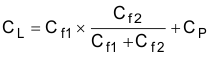
Table 6-5 lists the electrical characteristics of the clock crystal.

Table 6-5 Crystal Electrical Characteristics (Oscillator Mode)
NAMEDESCRIPTIONMINTYPMAXUNIT
fPParallel resonance crystal frequency40MHz
CLCrystal load capacitance5812pF
ESRCrystal ESR50Ω
Temperature rangeExpected temperature range of operation–40140°C
Frequency toleranceCrystal frequency tolerance(1)(2)–200200ppm
Drive level50200µW
The crystal manufacturer's specification must satisfy this requirement.
Includes initial tolerance of the crystal, drift over temperature, aging and frequency pulling due to incorrect load capacitance.
Table 6-6 External Clock Mode Specifications
PARAMETERSPECIFICATIONUNIT
MINTYPMAX
Input Clock:
External AC-coupled sine wave or DC-coupled square wave
Phase Noise referred to 40 MHz
Frequency40MHz
AC-Amplitude7001200adc patmV (pp)
Phase Noise at 1 kHz–132dBc/Hz
Phase Noise at 10 kHz–143dBc/Hz
Phase Noise at 100 kHz–152dBc/Hz
Phase Noise at 1 MHz–153dBc/Hz
Duty Cycle3565%
Freq Tolerance–100100ppm