ZHCS339E August 2010 – June 2019 AFE031
PRODUCTION DATA.
- 1 特性
- 2 应用
- 3 说明
- 4 修订历史记录
- 5 说明(续)
- 6 Device Comparison Table
- 7 Pin Configuration and Functions
-
8 Specifications
- 8.1 Absolute Maximum Ratings
- 8.2 ESD Ratings
- 8.3 Thermal Information
- 8.4 Electrical Characteristics: Transmitter (Tx)
- 8.5 Electrical Characteristics: Power Amplifier (PA)
- 8.6 Electrical Characteristics: Receiver (Rx)
- 8.7 Electrical Characteristics: Digital
- 8.8 Electrical Characteristics: Two-Wire Interface
- 8.9 Electrical Characteristics: Internal Bias Generator
- 8.10 Electrical Characteristics: Power Supply
- 8.11 Timing Requirements
- 8.12 Timing Diagrams
- 8.13 Typical Characteristics
- 9 Detailed Description
- 10Application and Implementation
- 11器件和文档支持
- 12机械、封装和可订购信息
9.2.4 DAC Block
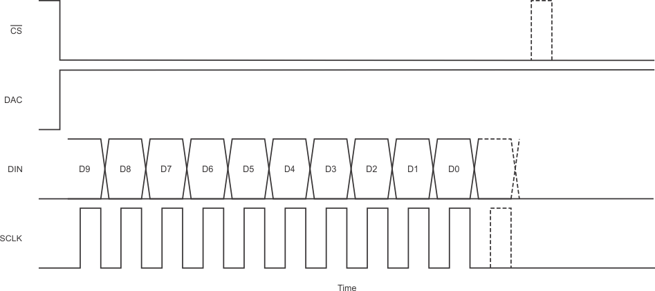
The DAC block consists only of the 10-bit DAC. The use of the DAC is recommended for best performance. The serial interface is used to write directly to the DAC registers when the DAC pin (pin 7) is driven high. Placing the DAC pin into a high state configures the SPI for direct serial interface to the DAC. Use the following sequence to write to the DAC:
- Set CS low.
- Set the DAC pin (pin 7) high.
- Write a 10-bit word to DIN. The DAC register is left-justified and truncates more than 10 bits.
- CS high updates the DAC.
Refer to Figure 34 for an illustration of this sequence.

NOINDENT:
NOTE: Dashed lines indicate optional additional clocks (data are ignored).Table 6 lists the DAC Register configurations.
Table 6. DAC Registers
| DAC PIN HIGH:
DAC REGISTER <15:0> |
LOCATION
(0 = LSB) |
DEFAULT | R/W | FUNCTION |
|---|---|---|---|---|
| BIT NAME | ||||
| DAC<0> | 0 | -- | W | Truncated |
| DAC<1> | 1 | -- | W | Truncated |
| DAC<2> | 2 | -- | W | Truncated |
| DAC<3> | 3 | -- | W | Truncated |
| DAC<4> | 4 | -- | W | Truncated |
| DAC<5> | 5 | -- | W | Truncated |
| DAC<6> | 6 | -- | W | DAC bit 0 = DAC LSB |
| DAC<7> | 7 | -- | W | DAC bit 1 |
| DAC<8> | 8 | -- | W | DAC bit 2 |
| DAC<9> | 9 | -- | W | DAC bit 3 |
| DAC<10> | 10 | -- | W | DAC bit 4 |
| DAC<11> | 11 | -- | W | DAC bit 5 |
| DAC<12> | 12 | -- | W | DAC bit 6 |
| DAC<13> | 13 | -- | W | DAC bit 7 |
| DAC<14> | 14 | -- | W | DAC bit 8 |
| DAC<15> | 15 | -- | W | DAC bit 9 = DAC MSB |