ZHCS339E August 2010 – June 2019 AFE031
PRODUCTION DATA.
- 1 特性
- 2 应用
- 3 说明
- 4 修订历史记录
- 5 说明(续)
- 6 Device Comparison Table
- 7 Pin Configuration and Functions
-
8 Specifications
- 8.1 Absolute Maximum Ratings
- 8.2 ESD Ratings
- 8.3 Thermal Information
- 8.4 Electrical Characteristics: Transmitter (Tx)
- 8.5 Electrical Characteristics: Power Amplifier (PA)
- 8.6 Electrical Characteristics: Receiver (Rx)
- 8.7 Electrical Characteristics: Digital
- 8.8 Electrical Characteristics: Two-Wire Interface
- 8.9 Electrical Characteristics: Internal Bias Generator
- 8.10 Electrical Characteristics: Power Supply
- 8.11 Timing Requirements
- 8.12 Timing Diagrams
- 8.13 Typical Characteristics
- 9 Detailed Description
- 10Application and Implementation
- 11器件和文档支持
- 12机械、封装和可订购信息
9.2.3 Rx Block
The Rx block consists of Rx PGA1, the Rx Filter, and Rx PGA2. Both Rx PGA1 and Rx PGA2 are high-performance programmable gain amplifiers. Rx PGA1 can be configured through the SPI to operate as either an attenuator or in gain. The gain steps of the Rx PGA1 are 0.25 V/V, 0.5 V/V, 1 V/V, and 2 V/V. The gain steps of the Rx PGA2 are 1 V/V, 4 V/V, 16 V/V, and 64 V/V. Configuring the Rx PGA1 as an attenuator (at gains less than 1 V/V) is useful for applications where the presence of large interference signals are present within the signal band. Attenuating the large interference allows these signals to pass through the analog Rx signal chain without causing an overload; the interference signal can then be processed and removed within the microprocessor as necessary.
The Rx Filter is a very low noise, unity-gain, fourth-order low-pass filter. The Rx Filter cutoff frequency is selectable between CENELEC A or CENELEC B, C, and D modes. The Control1 Register bit location 3 setting (CA CBCD) determines the cutoff frequency. Setting Control1 Register bit location 3 to '0' selects the CENELEC A band; setting Control1 Register bit location 3 to '1' selects the CENELEC B, C, and D bands. Because the Rx Filter is a very low noise analog filter, two external capacitors are required to properly configure the Rx Filter. Table 3 shows the proper capacitance values for CENELEC A, B, C, and D bands. Capacitor Rx C1 is connected between pin 24 and ground, and Rx C2 is connected between pin 23 and ground. For the capacitors shown, it is recommended that these components be rated to withstand the full AVDD power-supply voltage
Table 3. Recommended External Capacitors Required for Rx Filter
| FREQUENCY BAND | Rx C1, PIN 24 | Rx C2, PIN 23 | CUTOFF FREQUENCY (kHz) |
|---|---|---|---|
| CENELEC A | 680 pF | 680 pF | 90 |
| CENELEC B, C, D | 270 pF | 560 pF | 145 |
Figure 31 illustrates the recommended connections for the Rx signal chain.

As Figure 32 shows, a fourth-order passive passband filter is optional but recommended for applications where high performance is required. The external passive passband filter removes any unwanted, out-of-band signals from the signal path, and prevents them from reaching the active internal filters within the AFE031.

The following steps can be used to quickly design the passive passband filter. (Note that these steps produce an approximate result.)
- Choose the filter characteristic impedance, ZC:
- For –6-db passband attenuation: R1 = R2 = ZC
- For 0-db passband attenuation: R1 = ZC, R2 = 10 ● ZC
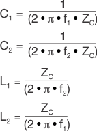
- Calculate values for C1, C2, L1, and L2 using the following equations:

Table 4 and Table 5 shows standard values for common applications.
Table 4. Recommended Component Values for Fourth-Order Passive Bandpass Filter (0-db Passband Attenuation)
| FREQUENCY BAND | FREQUENCY RANGE
(kHz) |
CHARACTERISTIC IMPEDANCE
(Ω) |
R1
(Ω) |
R2
(Ω) |
C1
(nF) |
C2
(nF) |
L1
(μH) |
L2
(μH) |
|---|---|---|---|---|---|---|---|---|
| CENELEC A | 35 to 95 | 1k | 1k | 10k | 4.7 | 1.5 | 1500 | 4700 |
| CENELEC B, C, D | 95 to 150 | 1k | 1k | 10k | 1.7 | 1 | 1200 | 1500 |
| SFSK | 63 to 74 | 1k | 1k | 10k | 2.7 | 2.2 | 2200 | 2200 |
Table 5. Recommended Component Values for Fourth-Order Passive Bandpass Filter (–6-db Passband Attenuation)
| FREQUENCY BAND | FREQUENCY RANGE
(kHz) |
CHARACTERISTIC IMPEDANCE
(Ω) |
R1
(Ω) |
R2
(Ω) |
C1
(nF) |
C2
(nF) |
L1
(μH) |
L2
(μH) |
|---|---|---|---|---|---|---|---|---|
| CENELEC A | 35 to 95 | 1k | 1k | 1k | 4.7 | 1.5 | 1500 | 4700 |
| CENELEC B, C, D | 95 to 150 | 1k | 1k | 1k | 1.7 | 1 | 1200 | 1500 |
| SFSK | 63 to 74 | 1k | 1k | 1k | 2.7 | 2.2 | 2200 | 2200 |
The Rx PGA1, Rx Filter, and Rx PGA2 components have all inputs and outputs externally available to provide maximum system design flexibility. Care should be taken when laying out the PCB traces from the inputs or outputs to avoid excessive capacitive loading. Keeping the PCB capacitance from the inputs to ground, or outputs to ground, below 100 pF is recommended.
Figure 33 shows the complete Rx signal path, including the optional passive passband filter.
