ZHCSBH3C May   2013  – March 2019 ADS8866

PRODUCTION DATA.  

  1. 特性
  2. 应用
  3. 说明
    1.     Device Images
      1.      ADC 电源无需独立的 LDO
  4. 修订历史记录
  5. Device Comparison Table
  6. Pin Configuration and Functions
    1.     Pin Functions
  7. Specifications
    1. 7.1 Absolute Maximum Ratings
    2. 7.2 ESD Ratings
    3. 7.3 Recommended Operating Conditions
    4. 7.4 Thermal Information
    5. 7.5 Electrical Characteristics
    6. 7.6 Timing Requirements: 3-Wire Operation
    7. 7.7 Timing Requirements: 4-Wire Operation
    8. 7.8 Timing Requirements: Daisy-Chain
    9. 7.9 Typical Characteristics
  8. Parameter Measurement Information
    1. 8.1 Equivalent Circuits
  9. Detailed Description
    1. 9.1 Overview
    2. 9.2 Functional Block Diagram
    3. 9.3 Feature Description
      1. 9.3.1 Analog Input
      2. 9.3.2 Reference
      3. 9.3.3 Clock
      4. 9.3.4 ADC Transfer Function
    4. 9.4 Device Functional Modes
      1. 9.4.1 CS Mode
        1. 9.4.1.1 3-Wire CS Mode
        2. 9.4.1.2 4-Wire CS Mode
      2. 9.4.2 Daisy-Chain Mode
        1. 9.4.2.1 Daisy-Chain Mode
  10. 10Application and Implementation
    1. 10.1 Application Information
      1. 10.1.1 ADC Reference Driver
      2. 10.1.2 ADC Input Driver
        1. 10.1.2.1 Input Amplifier Selection
        2. 10.1.2.2 Charge-Kickback Filter
    2. 10.2 Typical Applications
      1. 10.2.1 DAQ Circuit for a 10-µs, Full-Scale Step Response
        1. 10.2.1.1 Design Requirements
        2. 10.2.1.2 Detailed Design Procedure
      2. 10.2.2 DAQ Circuit for Lowest Distortion and Noise Performance at 100 kSPS
        1. 10.2.2.1 Design Requirements
        2. 10.2.2.2 Detailed Design Procedure
      3. 10.2.3 Ultralow-Power DAQ Circuit at 10 kSPS
        1. 10.2.3.1 Design Requirements
        2. 10.2.3.2 Detailed Design Procedure
  11. 11Power Supply Recommendations
    1. 11.1 Power-Supply Decoupling
    2. 11.2 Power Saving
  12. 12Layout
    1. 12.1 Layout Guidelines
    2. 12.2 Layout Example
  13. 13器件和文档支持
    1. 13.1 文档支持
      1. 13.1.1 相关文档
    2. 13.2 接收文档更新通知
    3. 13.3 社区资源
    4. 13.4 商标
    5. 13.5 静电放电警告
    6. 13.6 术语表
  14. 14机械、封装和可订购信息

封装选项

机械数据 (封装 | 引脚)
散热焊盘机械数据 (封装 | 引脚)
订购信息

Power Saving

The device has an auto power-down feature that powers down the internal circuitry at the end of every conversion. Referring to Figure 56, the input signal is acquired on the sampling capacitors when the device is in a power-down state (tacq); at the same time, the result for the previous conversion is available for reading. The device powers up on the start of the next conversion. During conversion phase (tconv), the device also consumes current from the reference source (connected to the REF pin).
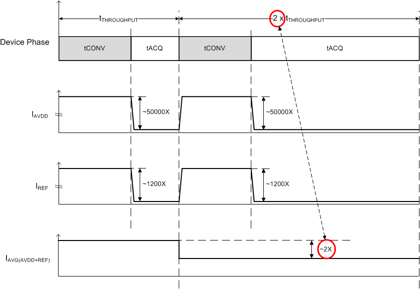
ADS8866 power_scaling_illustration.gifFigure 56. Power Scaling With Throughput

The conversion time, tconv, is independent of the SCLK frequency. When operating the device at speeds lower than the maximum rated throughput, the conversion time, tconv, does not change; the device spends more time in power-down state. Therefore, as shown in Figure 57, the device power consumption from the AVDD supply and the external reference source is directly proportional to the speed of operation. Extremely low AVDD power-down current (50 nA, typical) and extremely low external reference leakage current (250 nA, typical), make this device ideal for very low throughput applications (such as pulsed measurements).
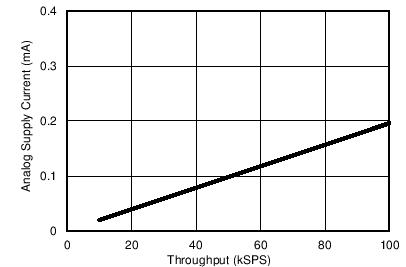
ADS8866 C003_SBAS614.pngFigure 57. Power Scaling With Throughput